Table 8-158, Dmc base spi ls word data register, Table 8-159 – Artesyn ATCA-8310 Installation and Use (May 2014) User Manual
Page 346: Dmc base spi ms word data register, Table 8-160, Dmc 1 spi control register, Cpld and fpga, 38 dmc 1 spi access registers
CPLD and FPGA
ATCA-8310 Installation and Use (6806800M72E)
346
8.2.2.3.38 DMC 1 SPI Access Registers
A write access to the DMC 1 SPI Control Register start the corresponding SPI access.
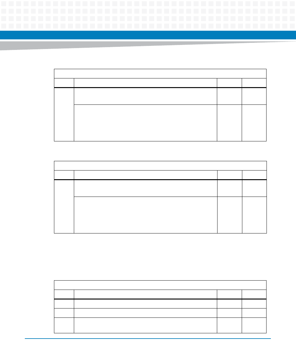
Table 8-158 DMC Base SPI LS Word Data Register
Address: 0xBA -0xBB
Bit Description
Default
Access
15:0
DMC Base SPI LS Word Write Data Register.
Contains the write bits 15:0 for a DMC register write access
-
SPP: w
DMC Base SPI LS Word Read Data Register.
Contains the data bits 15:0 of the selected DMC 32 bit register
when the DMC SPI access has terminated successfully.
Note: Read DMC Base SPI LS Word Data Register content as long SPI
access not started.
0
SPP: r
Table 8-159 DMC Base SPI MS Word Data Register
Address: 0xBC -0xBD
Bit Description
Default
Access
15:0
DMC Base SPI MS Word Write Data Register.
Contains the write bits 31:16 for a DMC register write access
-
SPP: w
DMC Base SPI MS Word Read Data Register.
Contains the data bits 31:16 of the selected DMC 32 bit register
when the DMC SPI access has terminated successfully.
Note: Read DMC Base SPI MS Word Data Register content as long
SPI access not started.
0
SPP: r
Table 8-160 DMC 1 SPI Control Register
Address: 0xC0 -0xC1
Bit Description
Default
Access
1:0
Reserved
0
r
7:2
DMC 1 address. Selects a 32 bit DMC register.
0
SPP: r/w
11:8
DMC 1 Byte Select. When the corresponding select bit is set the
corresponding byte of the selected DMC register can be accessed.
0
SPP: r/w