10 reset configuration – NEC Network Controller uPD98502 User Manual
Page 54
CHAPTER 1 INTRODUCTION
54
Preliminary User’s Manual S15543EJ1V0UM
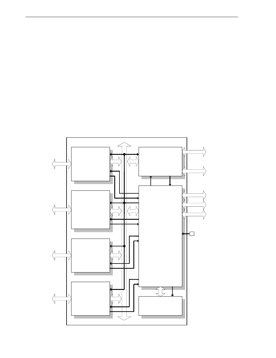
1.10 Reset Configuration
The falling edge of Clock Control Unit (CCU)’s reset line (RST_B) serves as the
µPD98502's internal reset. The
System Controller generates the IBUS reset signal using RST_B for the global reset of the
µPD98502. After 4 IBUS
clock (SDCLK), the System Controller deasserts the IBUS reset signal synchronously with IBUS clock (66 MHz). And
also the System Controller generates the internal Cold Reset signal and Hot Reset signal for performing the cold reset
of V
R
4120A. Once power to the
µPD98502 is established, the System Controller asserts internal CLKSET signal,
internal Cold Reset (COLDRST#) signal and internal Hot Reset (HOTRST#) signal at the falling edge of RST_B
signal. After 2 V
R
4120A clock (internal VCLOCK) cycles at rising edge of the RST_B, the System Controller deasserts
the CLKSET signal synchronously with “clkm”. Then 16 “clkm” cycles (see section 1.12) at the rising edge of the
RST_B signal, the System Controller deasserts the COLDRST# synchronously with “clkm”. And also the System
Controller deasserts the HOTRST# synchronously with “clkm” after 16 “clkm” clock cycles at deassertion of the
COLDRST#.
Figure 1-11. Reset Configuration
ATM Cell Processor
USB Controller
Ethernet
Controller
#1
System Controller
V
R
4120A RISC
Processor Core
µ
µ
µ
µ PD98502
RESET
ibrset
ibrset
ibrset
ibrset
reset
CLKSET
COLDRST#
HOTRST#
cresetb
macwrst
macwrst
usbwrst
usbwrst
atmwrst
atmwrst
macrdy
macrdy
usbrdy
atmrdy
atmrdy
usbrdy
Ethernet
Controller
#2
ibrset
mac2wrst
mac2rdy
mac2wrst
pcirdy
SDRAM
UTOPIA2
Boot ROM
USB
MII
MII
PHY-MGR
UART
IB
U
S
PCI
Controller
ibrset
pciwrst
pcirdy
pciwrst
mac2rdy
PCI