14 sdram – NEC Network Controller uPD98502 User Manual
Page 216
CHAPTER 3 SYSTEM CONTROLLER
216
Preliminary User’s Manual S15543EJ1V0UM
3.4.14 SDRAM
3.4.14.1 SDRAM address range
System memory can be populated with SDRAM chips, and it must have an access time of 10 ns or less. The
system controller supports 16-Mbit or 64-Mbit and 128-Mbit SDRAM at locations 0000_0000H through 01FF_FFFFH
in the physical memory space on V
R
4120A. The SDRAM supports V
R
4120A cache operations.
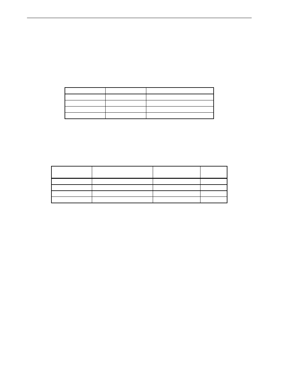
Table 3-8. SDRAM Size Configuration at Reset
SDMDR.SDS
SDRAM Size
Address Range
00
4 MB
0000_0000H through 003F_FFFH
01
8 MB
0000_0000H through 007F_FFFH
10
16 MB
0000_0000H through 00FF_FFFH
11
32 MB
0000_0000H through 01FF_FFFH
3.4.14.2 SDRAM device configurations
The controller supports the following 16-Mbit, 64-Mbit and 128-Mbit SDRAM organization. Following table indicates
some of the SDRAM organizations supported for system memory.
Table 3-9. SDRAM Configurations Supported
Memory Size
SMA Address Bits Required
Organization
(bank x word x bit)
Quantity
4 MB
12:0
2 x 0.5 M x 16
2
8 MB
12:0
4 x 0.5 M x 32
1
16 MB
13:0
4 x 1.0 M x 16
2
32 MB
13:0
4 x 2.0 M x 16
2
3.4.14.3 SDRAM burst-type and banks
The terms interleaved and bank have multiple meanings in the context of memory design using SDRAM chips. The
meanings are:
• Banks (applied to memory modules and SDRAM chips in different ways): The banks referenced with respect to
memory modules differ from the banks inside an SDRAM chip. For module, this controller does not support
what identifies their bank.
• Burst Type (applied to SDRAM chips): The burst type of a single SDRAM chip is programmed in the chip’s
mode register to be either interleaved or sequential. This concept relates only to the word order in which data
is read into and written out of the SDRAM chip. The concept does not relate to the number of words transferred
in a given clock cycle. The burst type for all SDRAM chips attached to the
µPD98502 is configured during the
memory initialization procedure. The memory controller in the system controller does not support the
interleaved burst mode and support only sequential burst mode.