NEC Network Controller uPD98502 User Manual
Page 214

CHAPTER 3 SYSTEM CONTROLLER
214
Preliminary User’s Manual S15543EJ1V0UM
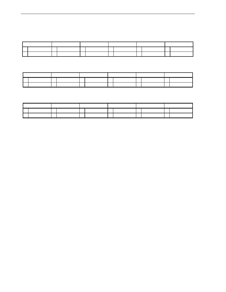
Table 3-7. Command Sequence
(a) Program Command Sequence (4 Write Cycles)
1st Write
2nd Write
3rd Write
4th Write
5th Write
6th Write
A
1FC0_2AA8H
A
1FC0_1554H
A
1FC0_2AA8H
A
PA*
A
A
D
AAAA_AAAAH
D
5555_5555H
D
A0A0_A0A0H
D
PD*
D
D
(b) Chip Erase Command Sequence (6 Write Cycles)
1st Write
2nd Write
3rd Write
4th Write
5th Write
6th Write
A
1FC0_2AA8H
A
1FC0_1554H
A
1FC0_2AA8H
A
1FC0_2AA8H
A
1FC0_1554H
A
1FC0_2AA8H
D
AAAA_AAAAH
D
5555_5555H
D
8080_8080H
D
AAAA_AAAAH
D
5555_5555H
D
1010_1010H
(c) Sector Erase Command Sequence (6 Write Cycles)
1st Write
2nd Write
3rd Write
4th Write
5th Write
6th Write
A
1FC0_2AA8H
A
1FC0_1554H
A
1FC0_2AA8H
A
1FC0_2AA8H
A
1FC0_1554H
A
EA*
D
AAAA_AAAAH
D
5555_5555H
D
8080_8080H
D
AAAA_AAAAH
D
5555_5555H
D
3030_3030H
Remark
A = memory write address
D = memory write data
PA = address of flash location to be programmed.
PD = data to be programmed at location PA.
EA = block address of flash location to be erased.
In case of Flash memory programming, please consider following system factors:
(1) Read cycle can’t interrupt these write commands. Therefore, it is impossible for the
µPD98502 to program Flash
memory with fetching from Flash memory.
(2) These write commands for Flash memory will be change on following system factors.
• Flash manufacturer company: Write sequences are differing among each company
• Endian mode (there are 3 system endian modes; Little endian, Big endian with data swap mode, and Big
endian with address swap mode)
• Flash data BUS size of Flash memory (ordinary Flash memory has both 8- and 16-bit BUS modes)
• Flash data BUS size of system controller (8, 16, 32 bits)
(3) Please make SMD and SMA signal outputs the same for write sequences.
