7 cache memory, 1 memory organization – NEC Network Controller uPD98502 User Manual
Page 168
CHAPTER 2 V
R
4120A
168
Preliminary User’s Manual S15543EJ1V0UM
2.7 Cache Memory
This section describes in detail the cache memory: its place in the V
R
4120A Core memory organization, and
individual organization of the caches.
2.7.1 Memory organization
Figure 2-65 shows the V
R
4120A Core system memory hierarchy. In the logical memory hierarchy, the caches lie
between the CPU and main memory. They are designed to make the speedup of memory accesses transparent to
the user.
Each functional block in Figure 2-65 has the capacity to hold more data than the block above it. For instance, main
memory (physical memory) has a larger capacity than the caches. At the same time, each functional block takes
longer to access than any block above it. For instance, it takes longer to access data in main memory than in the
CPU on-chip registers.
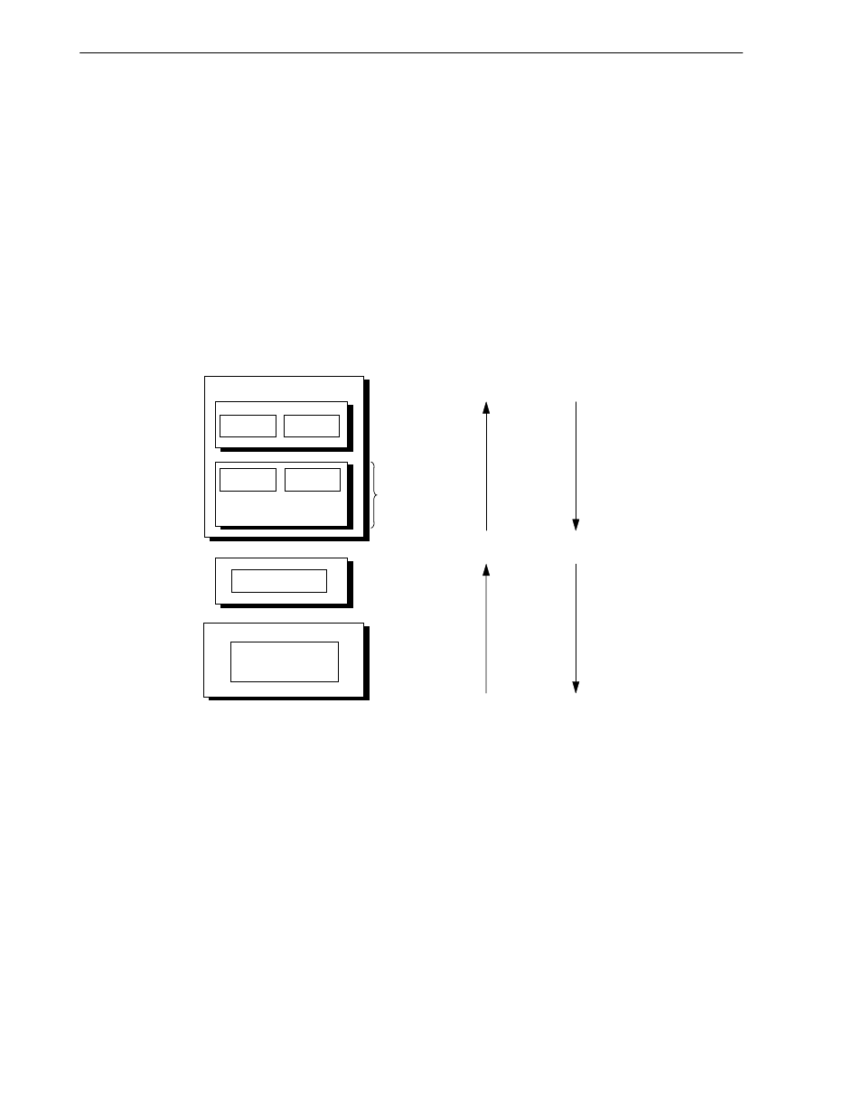
Figure 2-65. Logical Hierarchy of Memory
V
R
4120A CPU core
Register
Register
I-cache
D-cache
Cache
Main memory
Disc, CD-ROM,
tape, etc.
Register
Cache
Memory
Memory
media
Faster
access time
Increasing
data capacity
The V
R
4120A has two on-chip caches: one holds instructions (the instruction cache), the other holds data (the data
cache). The instruction and data caches can be read in one PClock cycle.
2 PCycles are needed to write data. However, data writes are pipelined and can complete at a rate of one per
PClock cycle. In the first stage of the cycle, the store address is translated and the tag is checked; in the second
stage, the data is written into the data RAM.