4 memory performance – NEC Network Controller uPD98502 User Manual
Page 206
CHAPTER 3 SYSTEM CONTROLLER
206
Preliminary User’s Manual S15543EJ1V0UM
3.4.4 Memory performance
The latency of memory accesses is determined by memory type, speed and prefetch scheme. Following lists some
examples of access latencies. 66-MHz or 100-MHz memory-bus clock is required for each transfer of a 4-word (16-
byte) CPU instruction-cache line fill. The first number in the “SysAD clocks” column is for the first word; the remaining
numbers are for the subsequent words. The most common combinations are shown.
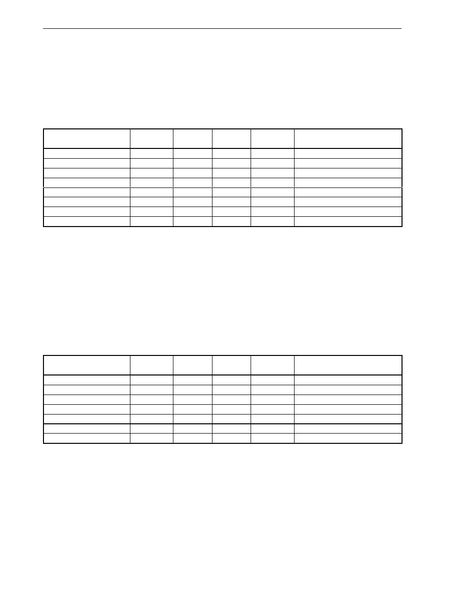
Table 3-4. Examples of Memory Performance (4-word-burst access from CPU)
Memory type
Bank-
interleaved
Page hit
R/W
Prefetch hit
Access latency view from CPU
[SysAD clocks]
SDRAM,10 ns
No
Yes
R
Yes
6-1-1-1
SDRAM,10 ns
No
Yes
R
No
14-1-1-1
SDRAM,10 ns
No
Yes
W
N/A
9-1-1-1
Flash, 85 ns (32-bit bus)
No
No
R
N/A
19-12-1-12
Flash, 85 ns (16-bit bus)
No
No
R
N/A
31-24-24-24
Flash, 85 ns (8-bit bus)
No
No
R
N/A
55-48-48-48
Flash, 85 ns
No
No
W
N/A
18 (single access only)
PROM
No
No
R
N/A
19-12-12-12
Remarks 1. SDRAM configuration: RCD = 3, CL = 2, SDCLK = 100 MHz, FAT = 10
2. BUS frequency: SysAD = 100 MHz, IBUS = 66 MHz
3. Read performance is calculated by counting the rising edge for CPU clock where the read command is
issued by the CPU. Because the CPU issues write data with no wait-states once the write command is
issued, the numbers in the table represent the rate at which data is written to memory. The sum of the
numbers represents the number of cycles between when the write operation was issued and when the
next CPU memory operation can begin.
4. The burst-write access to the flash/ROM is invalid. The CPU can access to the flash/ROM using single
access only
Table 3-5. Examples of Memory Performance (4-word-burst access from IBUS Master)
Memory type
Bank-
interleaved
Page hit
R/W
Prefetch hit
Access latency view from IBUS
[IBUS clocks]
SDRAM,10 ns
No
Yes
R
N/A
18-1-1-1
SDRAM,10 ns
No
Yes
W
N/A
12-1-1-1
Flash, 85 ns (32-bit bus)
No
No
R
N/A
45-1-1-1
Flash, 85 ns (16-bit bus)
No
No
R
N/A
77-1-1-1
Flash, 85 ns (8-bit bus)
No
No
R
N/A
141-1-1-1
Flash, 85 ns
No
No
W
N/A
Invalid
PROM
No
No
R
N/A
45-1-1-1
Remarks 1. SDRAM configuration: RCD = 3, CL = 2, SDCLK = 100 MHz, FAT = 10
2. BUS frequency: SysAD = 100 MHz, IBUS = 66 MHz
3. Above access latency doses not include the IBUS arbitration cycle (4 IBUS clocks).
4. Any write access to the flash/ROM is prohibited. If the IBUS master perform the write access to the
flash/ROM, The IBUS bus error will be occurred.