5 memory interface – NEC Network Controller uPD98502 User Manual
Page 39
CHAPTER 1 INTRODUCTION
Preliminary User’s Manual S15543EJ1V0UM
39
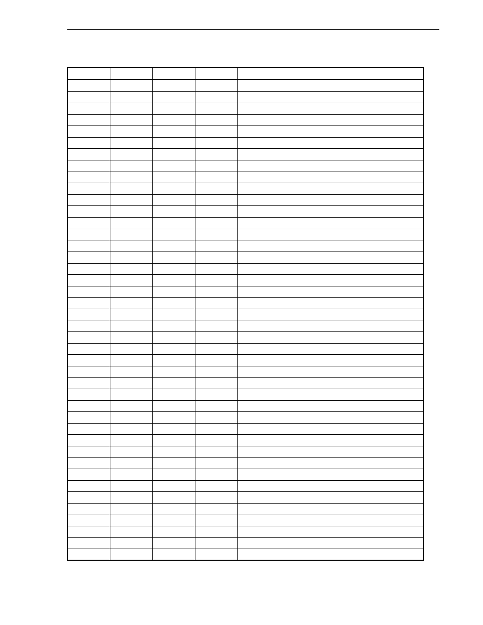
1.7.5 Memory interface
(1/2)
Pin Name
Pin No.
I/O
Active Level
Function
SDCLK0
L1
O
SDRAM clock
SDCLK1
G3
O
SDRAM clock
SDCKE0
L3
O
H
SDRAM clock enable
SDCKE1
F2
O
H
SDRAM clock enable
SDCS_B
F3
O
L
Chip select
SDRAS_B
E2
O
L
Row address strobe
SDCAS_B
G5
O
L
Column address strobe
SDWE_B
D1
O
L
Write enable
SRMCS_B
A7
O
L
PROM/FLASH chip select
SRMOE_B
C8
O
L
PROM/FLASH output enable
SMA0
E3
O
Memory address
SMA1
D2
O
Memory address
SMA2
C1
O
Memory address
SMA3
J2
O
Memory address
SMA4
H1
O
Memory address
SMA5
J3
O
Memory address
SMA6
J4
O
Memory address
SMA7
H2
O
Memory address
SMA8
G1
O
Memory address
SMA9
H3
O
Memory address
SMA10
E4
O
Memory address
SMA11
D3
O
Memory address
SMA12
B1
O
Memory address
SMA13
A1
O
Memory address
SMA14
B2
O
Memory address
SMA15
G2
O
Memory address
SMA16
C3
O
Memory address
SMA17
F1
O
Memory address
SMA18
J1
O
Memory address
SMA19
K3
O
Memory address
SMA20
K2
O
Memory address
SMD0
A2
I/O
Memory data
SMD1
B3
I/O
Memory data
SMD2
C4
I/O
Memory data
SMD3
D5
I/O
Memory data
SMD4
A3
I/O
Memory data
SMD5
B4
I/O
Memory data
SMD6
D6
I/O
Memory data
SMD7
A4
I/O
Memory data
SMD8
T1
I/O
Memory data
SMD9
R3
I/O
Memory data
SMD10
R4
I/O
Memory data