5 i2c parameter ram, I2com field descriptions -9, Wn in figure 34-10, is used to start i – Motorola MPC8260 User Manual
Page 951: C parameter ram, Table 34-5 describes i2com þelds, The i, C is inactive
MOTOROLA
Chapter 34. I2C Controller
34-9
Part IV. Communications Processor Module
Table 34-5 describes I2COM Þelds.
34.5 I
2
C Parameter RAM
The I
2
C controller parameter table is used for the general I
2
C parameters and is similar to
the SCC general-purpose parameter RAM. The CP accesses the I
2
C parameter table using
a user-programmed pointer (I2C_BASE) located in the parameter RAM; see
Section 13.5.2, ÒParameter RAM.Ó The I
2
C parameter table can be placed at any 64-byte
aligned address in the dual-port RAMÕs general-purpose area (banks #1Ð#8). The user must
initialize certain parameter RAM values before the I
2
C is enabled; the CP initializes the
other values. Software usually does not access parameter RAM entries once they are
initialized; they should be changed only when the I
2
C is inactive.
Bit
0
1
2
3
4
5
6
7
Field
STR
Ñ
M/S
Reset
0000_0000
R/W
R/W
Addr
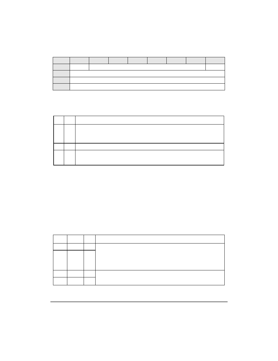
Figure 34-10. I
2
C Command Register (I2COM)
Table 34-5. I2COM Field Descriptions
Bits
Name Description
0
STR
Start transmit. In master mode, setting STR causes the I
2
C controller to start sending data from the
I
2
C Tx buffers if they are ready. In slave mode, setting STR when the I
2
C controller is idle causes it to
load the Tx data register from the I
2
C Tx buffer and start sending when it receives an address byte that
matches the slave address with R/W = 1. STR is always read as a 0.
1Р6
С
Reserved and should be cleared.
7
M/S
Master/slave. ConÞgures the I
2
C controller to operate as a master or a slave.
0 I
2
C is a slave.
1 I
2
C is a master.
Table 34-6. I
2
C Parameter RAM Memory Map
Offset
1
Name
Width
Description
0x00
RBASE
Hword Rx/TxBD table base address. Indicate where the BD tables begin in the dual-port RAM.
Setting Rx/TxBD[W] in the last BD in each BD table determines how many BDs are
allocated for the Tx and Rx sections of the I
2
C. Initialize RBASE/TBASE before enabling
the I
2
C. Furthermore, do not conÞgure BD tables of the I
2
C to overlap any other active
controllerÕs parameter RAM.
RBASE and TBASE should be divisible by eight.
0x02
TBASE
Hword
0x04
RFCR
Byte
Rx/Tx function code registers. The function code registers contain the transaction
speciÞcation associated with SDMA channel accesses to external memory. See
Figure 34-11 and Table 34-7.
0x05
TFCR
Byte