10 basic power structure, Basic power structure -10, Relationships of scmr parameters -10 – Motorola MPC8260 User Manual
Page 276
9-10
MPC8260 PowerQUICC II UserÕs Manual
MOTOROLA
Part III. The Hardware Interface
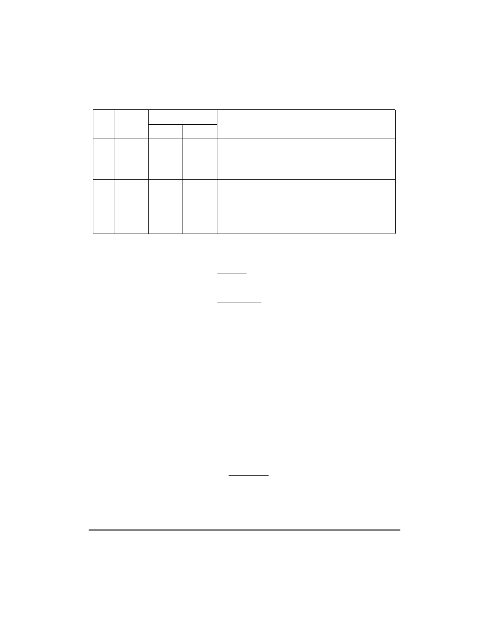
The relationships among these parameters are described in the formulas in Figure 9-5.
Figure 9-5. Relationships of SCMR Parameters
9.10 Basic Power Structure
The I/O buffers, logic, and clock block are fed by a 3.3-V power supply that allows them to
function in a TTL-compatible voltage range. Internal logic can be fed by a 2.0-V source
considerably reducing power consumption. The PLL is fed by a separate power supply
(VCCSYN) to achieve a highly stable output frequency. The VCCSYN value is equal to the
internal supply (2.0 V).
The MPC8260 supports the two following power modes:
¥
Full mode: Both the chip PLL and core PLL work.
¥
Stop mode: Main PLL is working, core PLL is stopped, internal clocks are disabled.
Ñ When stop mode is entered, software sets the sleep bit in the core (HID0[10] =
1) and the clock block freezes all clocks to the chip (the core clock and all other
clocks) the main PLL remains active
Ñ When stop mode is exited, the SRESET_B input must be asserted to the chip, the
clock block resumes clocks to all blocks and then releases the reset to the whole
chip.
19
PLLDF
ConÞg pins
Unaffected
PLL pre-divider value. Ensures that PLLMF is an integer value
regardless of whether CPM_CLK/CLKIN is an integer.
0 The ratio, CPM_CLK/CLKIN, is an integer
1 The ratio, CPM_CLK/CLKIN, is not an integer
PLL division factor can be either 1 or 2.
20Ð31
PLLMF
ConÞg pins
Unaffected
PLL multiplication factor. (A PLLMF value of 0x000 corresponds to 1,
and 0xFFF to 4,096.) The VCO output is divided to generate the
feedback signal that goes to the phase comparator. PLLMF and
PLLDF bits control the value of the divider in the PLL feedback loop.
The phase comparator determines the phase shift between the
feedback signal and the reference clock. This difference causes an
increase or decrease in the VCO output frequency.
Table 9-5. SCMR Field Descriptions (Continued)
Bits
Name
Defaults
Description
POR
Hard Reset
PLLMF = CPM_CLK
CLKIN
´
(PLLDF + 1) Ð 1
BUSDF = (PLLMF + 1)
´
2
(PLLDF + 1)
Р 1