3 nmsi configuration, Nmsi configuration -4, Enabling connections to the tsa -4 – Motorola MPC8260 User Manual
Page 494: 3 nmsi conþguration

15-4
MPC8260 PowerQUICC II UserÕs Manual
MOTOROLA
Part IV. Communications Processor Module
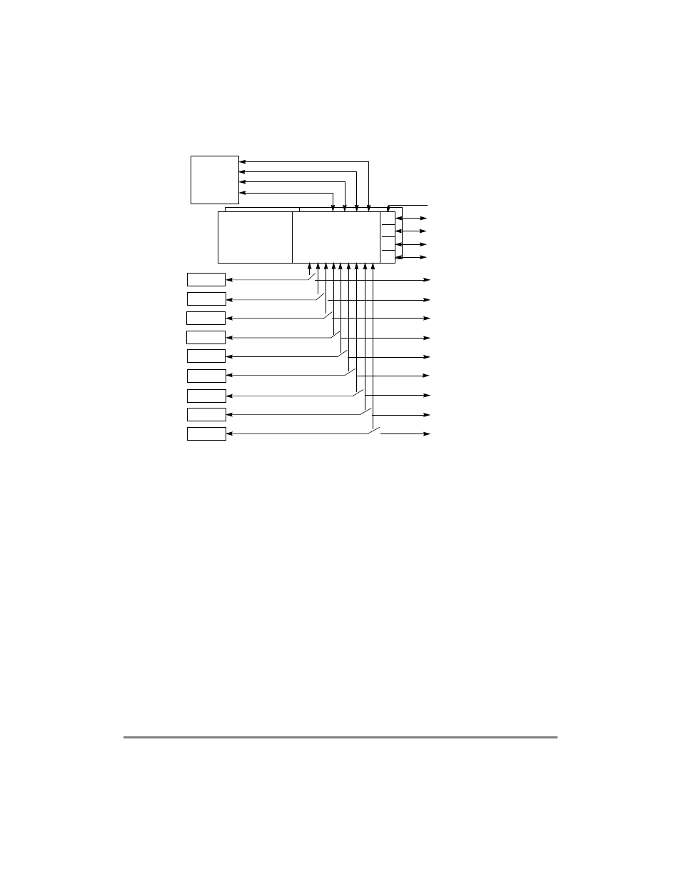
Figure 15-2. Enabling Connections to the TSA
15.3 NMSI ConÞguration
The CMX supports an NMSI mode for each of the FCCs, SCCs, and SMCs. Each serial
device is connected independently either to the NMSI or to the TSA using the clock route
registers. The user should note, however, that NMSI pins are multiplexed with other
functions at the parallel I/O lines. Therefore, if a combination of TDM and NMSI channels
are used, consult the MPC8260Õs pinout to determine which FCC, SCC, and SMC to
connect and where to connect them.
The clocks provided to the FCCs, SCCs, and SMCs are derived from a bank of 8 internal
BRGs and 20 external CLK pins; see Figure 15-3. There are two main advantages to the
bank-of-clocks approach. First, a serial device is not forced to choose a serial device clock
from a predeÞned pin or BRG; this allows a ßexible pinout-mapping strategy. Second, a
group of serial receivers and transmitters that needs the same clock rate can share the same
pin. This conÞguration leaves additional pins for other functions and minimizes potential
skew between multiple clock sources.
En
En
En
En
SI RAMs
Time-Slot
Assigners
TDM a,b,c,d Enable = 1
TDM a Pins
TDM b Pins
TDM c Pins
TDM d Pins
FCC1
FCC2
FCC3
SCC1
SCC2
SCC3
SCC4
SMC1
SMC2
MII1/UTOPIA 8/16/M-phy
FC1 = 0
MII2/UTOPIA 8/M-phy
FC2 = 0
MII3
FC3 = 0
SCC1 Pins
SC1 = 0
SCC2 Pins
SC2 = 0
SCC3 Pins
SC3 = 0
SCC4 Pins
SC4 = 0
SMC1 Pins
SMC1 = 0
SMC2 Pins
SMC2 = 0
MCCs
TDM a channels
TDM b channels
TDM c channels
TDM d channels
NMSI Mode
