Motorola MPC8260 User Manual
Page 332

10-56
MPC8260 PowerQUICC II UserÕs Manual
MOTOROLA
Part III. The Hardware Interface
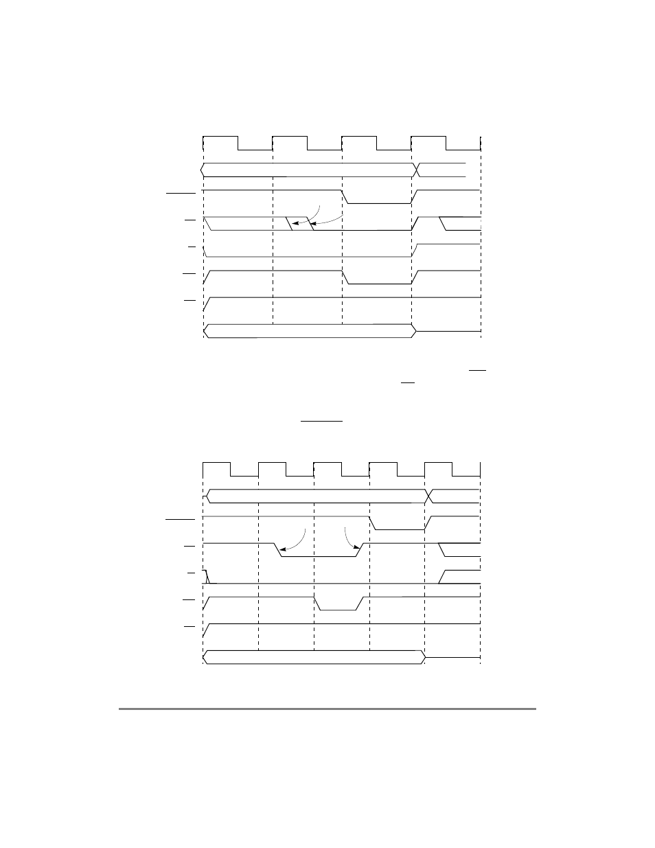
Figure 10-47. GPCM Relaxed-Timing Write (ACS = 1x, SCY = 0, CSNT = 0,TRLX = 1)
When TRLX and CSNT are set in a write-memory access, the strobe lines, WE[0Ð7] are
negated one clock earlier than in the normal case. If ACS
¹ 0, CS is also negated one clock
earlier, as shown in Figure 10-48 and Figure 10-49. When a bank is selected to operate with
external transfer acknowledge (SETA and TRLX = 1), the memory controller does not
support external devices that provide PSDVAL to complete the transfer with zero wait
states. The minimum access duration in this case is three clock cycles.
Figure 10-48
.
GPCM Relaxed-Timing Write (ACS = 10, SCY = 0, CSNT = 1, TRLX = 1)
Clock
Address
PSDVAL
CS
R/W
WE
OE
Data
ACS = 10
ACS = 11
Clock
Address
PSDVAL
CS
R/W
WE
OE
Data
ACS = 10
CSNT = 1
- SB5101U DOCSIS 2.0 Cable Modem (16 pages)
- PTP 500 (20 pages)
- Netopia 3347-02-ENT (3 pages)
- SBV5220 (64 pages)
- AP-51XX (698 pages)
- SURFboard SVG2501 Series (34 pages)
- MESH Wireless Router MWR6300 (2 pages)
- MVME712AM (74 pages)
- SURFBOARD SBG1000 (16 pages)
- RSGu3502 (5 pages)
- SURFboard SBG941U (78 pages)
- Netopia 2240N-VGx (5 pages)
- SURFboard SVG2501 (8 pages)
- WR850G (93 pages)
- WR850GP (95 pages)
- USBW 200 (12 pages)
- ONCE SC140 (28 pages)
- Netopia 3300 (368 pages)
- WNS25 (2 pages)
- Netopia 7000 (254 pages)
- Viadux 2000 Subscriber Bridge RC2010 (1 page)
- MVME5100 Series (5 pages)
- ColdFire MCF5282 (766 pages)
- MC9S12C-Family (136 pages)
- CG4500 (36 pages)
- SBG900 (130 pages)
- SURFBOARD SB5100 (2 pages)
- SURFboard SB6180 (20 pages)
- SURFBOARD SBG900 (16 pages)
- SURFboard SVG1501U (83 pages)
- SB5100 (74 pages)
- T3 (2 pages)
- H375 (5 pages)
- NETOPIA 2247/57-62 (22 pages)
- SBV5120 (57 pages)
- SBV5120 (56 pages)
- RG2200 (88 pages)
- CME-12B/BC (18 pages)
- SURFboard 574823-001-a (2 pages)
- SURFboard Cable Modem (66 pages)
- CME-12D60 (19 pages)
- DIGITAL VOICE MODEM SBV5122 (24 pages)
- SB4000 (2 pages)
- Canopy FSK and OFDM radios PTP 200 (OFDM (56 pages)
