Output control cell (io.ctl) -5, General arrangement of bidirectional pin cells -5 – Motorola MPC8260 User Manual
Page 397
MOTOROLA
Chapter 12. IEEE 1149.1 Test Access Port
12-5
Part III. The Hardware Interface
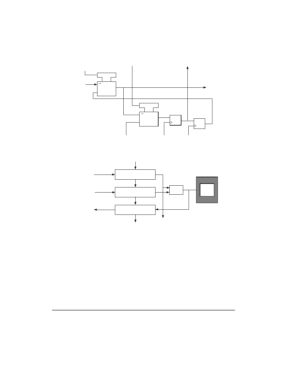
Figure 12-5. Output Control Cell (IO.CTL)
Figure 12-6. General Arrangement of Bidirectional Pin Cells
The control bit value controls the output function of the bidirectional pin. One or more
bidirectional data cells can be serially connected to a control cell. Bidirectional pins include
two scan cell for data (IO.Cell) as shown in Figure 12-6 and these bits are controlled by the
cell shown in Figure 12-5.
It is important to know the boundary scan bit order and pins that are associated with them.
Table 12-2 shows the bit order starting with the TDO output and ending with the TDI input.
The Þrst column of the table deÞnes the bitÕs ordinal position in the boundary scan register.
The shift register cell nearest TDO (Þrst to be shifted in) is deÞned as Bit 1 and the last bit
to be shifted in is bit 475. The second column references one of the three MPC8260Õs cell
types depicted in Figure 12-3 through Figure 12-5 that describe the cell structure for each
1
1
MUX
G1
1
1
MUX
G1
C
D
C
D
From Last Cell
Clock DR
Update DR
Shift DR
1 Ñ EXTEST | Clamp
To Output
Buffer
0 Ñ Otherwise
To Next Cell
Output Control
Logic
from System
I/O
Pin
From Last Cell
Output Data
Input Data
Output Enable
I.OBS
EN
from System Logic
O.PIN
I/O.CTL
To Next Pin Pair
To Next Cell