2 protocol-specific mode register (psmr), 3 data synchronization register (dsr), 4 transmit-on-demand register (todr) – Motorola MPC8260 User Manual
Page 565: Protocol-specific mode register (psmr) -9, Data synchronization register (dsr) -9, Transmit-on-demand register (todr) -9, 2 protocol-speciþc mode register (psmr)

MOTOROLA
Chapter 19. Serial Communications Controllers (SCCs)
19-9
Part IV. Communications Processor Module
19.1.2 Protocol-SpeciÞc Mode Register (PSMR)
The protocol implemented by an SCC is selected by its GSMR_L[MODE]. Each SCC has
an additional protocol-speciÞc mode register (PSMR) that conÞgures it speciÞcally for the
chosen protocol. The PSMR Þelds are described in the speciÞc chapters that describe each
protocol. PSMRs are cleared at reset. PSMRs reside at the following addresses: 0x11A08
(PSMR1), 0x11A28 (PSMR2), 0x11A48 (PSMR3), and 0x11A68 (PSMR4).
19.1.3 Data Synchronization Register (DSR)
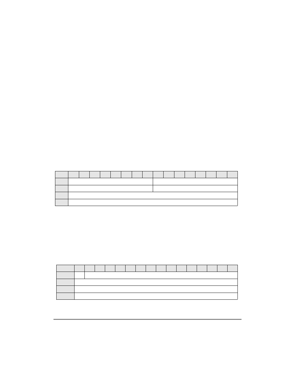
Each SCC has a data synchronization register (DSR) that speciÞes the pattern used for
frame synchronization. The programmed value for DSR depends on the protocol:
¥
UARTÑDSR is used to conÞgure fractional stop bit transmission.
¥
BISYNC and transparentÑDSR should be programmed with the sync pattern.
¥
EthernetÑDSR should be programmed with 0xD555.
¥
HDLCÑAt reset, DSR defaults to 0x7E7E (two HDLC ßags), so it does not need to
be written.
Figure 19-4 shows the sync Þelds.
19.1.4 Transmit-on-Demand Register (TODR)
In normal operation, if no frame is being sent by an SCC, the CP periodically polls the R
bit of the next TxBD to see if a new frame/buffer is requested. Depending on the SCC
conÞguration, this polling occurs every 8Ð32 serial Tx clocks. The transmit-on-demand
option, selected in the transmit-on-demand register (TODR) shown in Figure 19-5,
shortens the latency of the Tx buffer/frame and is useful in LAN-type protocols where
maximum inter-frame gap times are limited by the protocol speciÞcation.
Bit
0
1
2
3
4
5
6
7
8
9
10
11
12
13
14
15
Field
SYN2
SYN1
Reset
0111_1110
0111_1110
R/W
R/W
Addr
0x11A0E (DSR1); 0x11A2E (DSR2); 0x11A4E (DSR3); 0x11A6E (DSR4)
Figure 19-4. Data Synchronization Register (DSR)
Bit
0
1
2
3
4
5
6
7
8
9
10
11
12
13
14
15
Field
TOD
Ñ
Reset
0000_0000_0000_0000
R/W
R/W
Addr
0x11A0C (TODR1); 0x11A2C (TODR2); 0x11A4C (TODR3); 0x11A6C (TODR4)
Figure 19-5. Transmit-on-Demand Register (TODR)
