2 command register example, 3 command execution latency, 5 dual-port ram – Motorola MPC8260 User Manual
Page 445: Command register example -15, Command execution latency -15, Dual-port ram -15, Dual-port ram block diagram -15
MOTOROLA
Chapter 13. Communications Processor Module Overview
13-15
Part IV. Communications Processor Module
13.4.2 Command Register Example
To perform a complete reset of the CP, the value 0x8001_0000 should be written to the
CPCR. Following this command, the CPCR returns the value 0x0000_0000 after two
clocks.
13.4.3 Command Execution Latency
The worst-case command execution latency is 200 clocks and the typical command
execution latency is about 40 clocks.
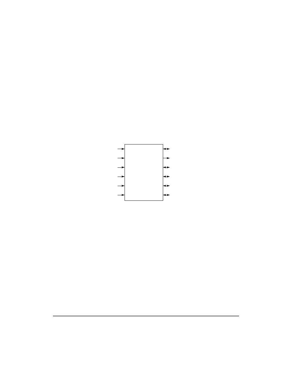
13.5 Dual-Port RAM
The CPM has 24 Kbytes of static RAM. Figure 13-7 is a block diagram of the dual-port
RAM.
Figure 13-7. Dual-Port RAM Block Diagram
The dual-port RAM can be accessed by the following:
¥
CP load/store unit
¥
CP block transfer module (BTM)
¥
CP instruction fetcher (when executing microcode from RAM)
¥
PowerPCª 60x slave
¥
SDMA 60x bus
¥
SDMA local bus
Figure 13-8 shows the memory map of the dual-port RAM.
Slave Address
CP Instruction Address
CP Data Address
24 KBytes
Dual-Port RAM
(BDs, Buffers
and Microcode)
DMA (60x) Address
DMA (Local) Address
BTM Address
Slave Data
CP Instruction
CP Data
DMA (60x) Data
DMA (Local) Data
BTM Data