3 smc parameter ram, Smc parameter ram -6 – Motorola MPC8260 User Manual
Page 702
26-6
MPC8260 PowerQUICC II UserÕs Manual
MOTOROLA
Part IV. Communications Processor Module
The BD table allows buffers to be deÞned for transmission and reception. Each table forms
a circular queue. The CP uses BDs to conÞrm reception and transmission so that the
processor knows buffers have been serviced. The data resides in external or internal buffers.
When SMCs are conÞgured to operate in GCI mode, their memory structure is predeÞned
to be one half-word long for transmit and one half-word long for receive. For more
information on these half-word structures, see Section 26.5, ÒThe SMC in GCI Mode.Ó
26.2.3 SMC Parameter RAM
The CP accesses each SMCÕs parameter table using a user-programmed pointer
(SMCx_BASE) located in the parameter RAM; see Section 13.5.2, ÒParameter RAM.Ó
Each SMC parameter RAM table can be placed at any 64-byte aligned address in the dual-
port RAMÕs general-purpose area (banks #1Ð#8). The protocol-speciÞc portions of the
SMC parameter RAM are discussed in the sections that follow. The SMC parameter RAM
shared by the UART and transparent protocols is shown in Table 26-2. Parameter RAM for
GCI protocol is described in Table 26-17.
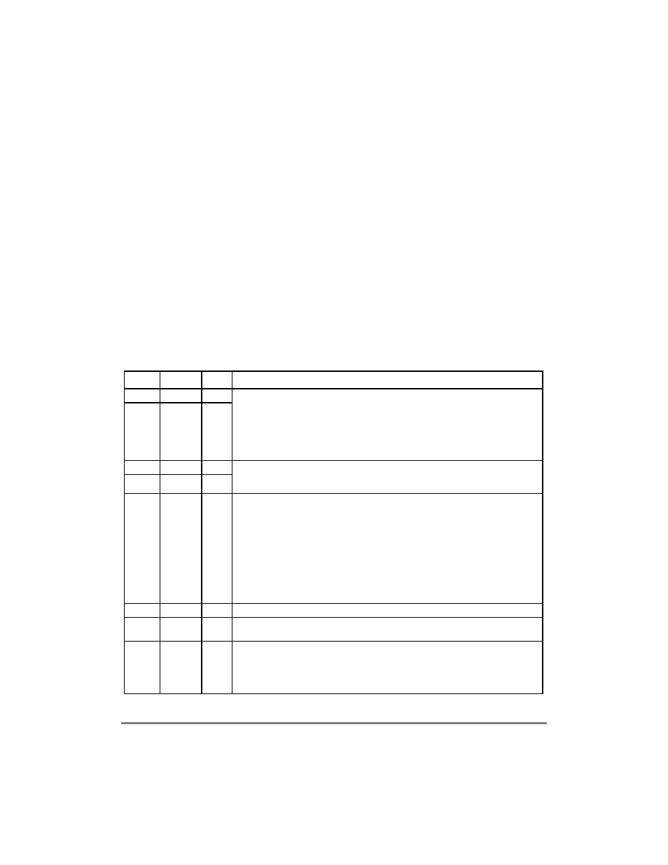
Table 26-2. SMC UART and Transparent Parameter RAM Memory Map
Offset
1
Name
Width
Description
0x00
RBASE
Hword
RxBDs and TxBDs base address. (BD table pointer) DeÞne starting points in the dual-
port RAM of the set of BDs for the SMC send and receive functions. They allow ßexible
partitioning of the BDs. By selecting RBASE and TBASE entries for all SMCs and by
setting W in the last BD in each list, BDs are allocated for the send and receive side of
every SMC. Initialize these entries before enabling the corresponding channel.
ConÞguring BD tables of two enabled SMCs to overlap causes erratic operation. RBASE
and TBASE should be a multiple of eight.
0x02
TBASE
Hword
0x04
RFCR
Byte
Rx/Tx function code. The two SMC channels have four RFCRs for receive data buffers
and four TFCRs for transmit data buffers. See Section 26.2.3.1, ÒSMC Function Code
Registers (RFCR/TFCR).Ó
0x05
TFCR
Byte
0x06
MRBLR
Hword
Maximum receive buffer length. The most bytes the MPC8260 writes to a receive buffer
before moving to the next buffer. It can write fewer bytes than MRBLR if a condition like
an error or end-of-frame occurs, but it cannot exceed MRBLR. MPC8260 buffers should
not be smaller than MRBLR. SMC transmit buffers are unaffected by MRBLR.
Transmit buffers can be individually given varying lengths through the data length Þeld.
MRBLR can be changed while an SMC is operating only if it is done in a single bus cycle
with one 16-bit move (not two 8-bit bus cycles back-to-back). This occurs when the CP
shifts control to the next RxBD, so the change does not take effect immediately. To
guarantee the exact RxBD on which the change occurs, change MRBLR only while the
SMC receiver is disabled. MRBLR should be greater than zero and should be even if
character length exceeds 8 bits.
0x08
RSTATE
Word
Can be used only by the CP.
0x0C
Ñ
Word
Rx internal data pointer.
2
Updated by the SDMA channels to show the next address in
the buffer to be accessed.
0x10
RBPTR
Hword RxBD pointer. Points to the next BD for each SMC channel that the receiver transfers
data to when it is in idle state, or to the current BD during frame processing. After a reset
or when the end of the BD table is reached, the CP initializes RBPTR to the value in
RBASE. Most applications never need to write RBPTR, but it can be written when the
receiver is disabled or when no receive buffer is in use.