One-clock delay from sync to data (xfsd = 01) -20, No delay from sync to data (xfsd = 00) -20, Figure 14-12 and figure 14-13 sho – Motorola MPC8260 User Manual
Page 474: See figure 14-13, figure 14-14
14-20
MPC8260 PowerQUICC II UserÕs Manual
MOTOROLA
Part IV. Communications Processor Module
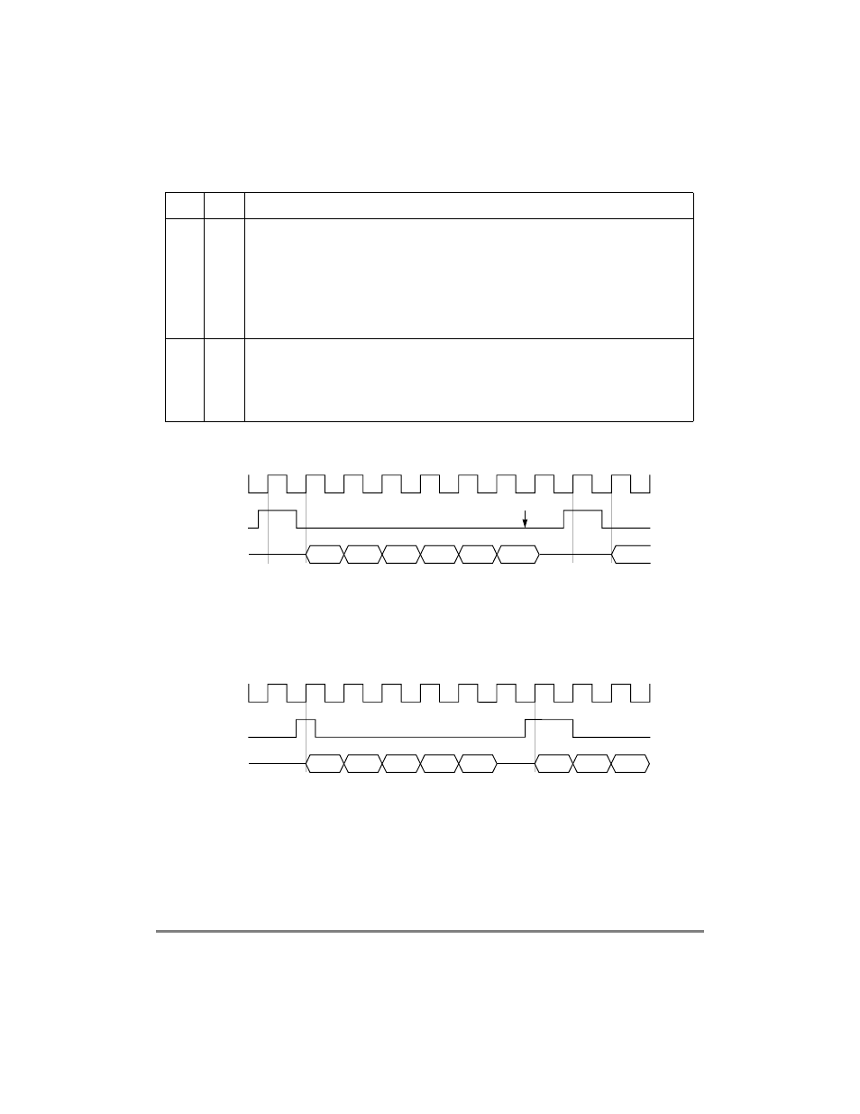
Figure 14-12 shows the one-clock delay from sync to data when xFSD = 01.
Figure 14-12. One-Clock Delay from Sync to Data (xFSD = 01)
Figure 14-13 shows the elimination of the single-clock delay shown in Figure 14-12 by
clearing xFSD.
Figure 14-13. No Delay from Sync to Data (xFSD = 00)
13
GMx
Grant mode for TDM a, b, c or d
0 GCI/SCIT mode. The GCI/SCIT D channel grant mechanism for transmission is internally
supported. The grant is one bit from the receive channel. This bit is marked by programming the
channel select bits of the SIx RAM with 0111 to assert an internal strobe on it. See
Section 14.7.2.2, ÒSCIT Programming.Ó
1 IDL mode. A grant mechanism is supported if the corresponding CMXSCR[GRx] bit is set. The
grant is a sample of L1GRx while L1TSYNCx is asserted. This grant mechanism implies the IDL
access controls for transmission on the D channel. See Section 14.6.2, ÒIDL Interface
Programming.У
14Р15
TFSDx Transmit frame sync delay for TDM a, b, c or d. Determines the number of clock delays between the
transmit sync and the Þrst bit of the transmit frame. See Figure 14-16.
00 No bit delay. The Þrst bit of the frame is transmitted/received on the same clock as the sync.
01 1-bit delay
10 2-bit delay
11 3-bit delay
Table 14-5. SIxMR Field Descriptions (Continued)
Bits
Name
Description
L1CLK
Data
(CE=0)
L1SYNC
(FE=1)
Bit-0
Bit-1
Bit-2
Bit-3
Bit-4
Bit-0
One-Clock Delay from Sync Latch to First Bit of Frame
Bit-5
End of Frame
L1CLK
Data
(CE=0)
L1SYNC
(FE=1)
Bit-0
Bit-1
Bit-2
Bit-3
Bit-4
No Delay from Sync Latch to First Bit of Frame
Bit-2
Bit-1
Bit-0