1 features, Features -2, Cpm multiplexing logic (cmx) block diagram -2 – Motorola MPC8260 User Manual
Page 492

15-2
MPC8260 PowerQUICC II UserÕs Manual
MOTOROLA
Part IV. Communications Processor Module
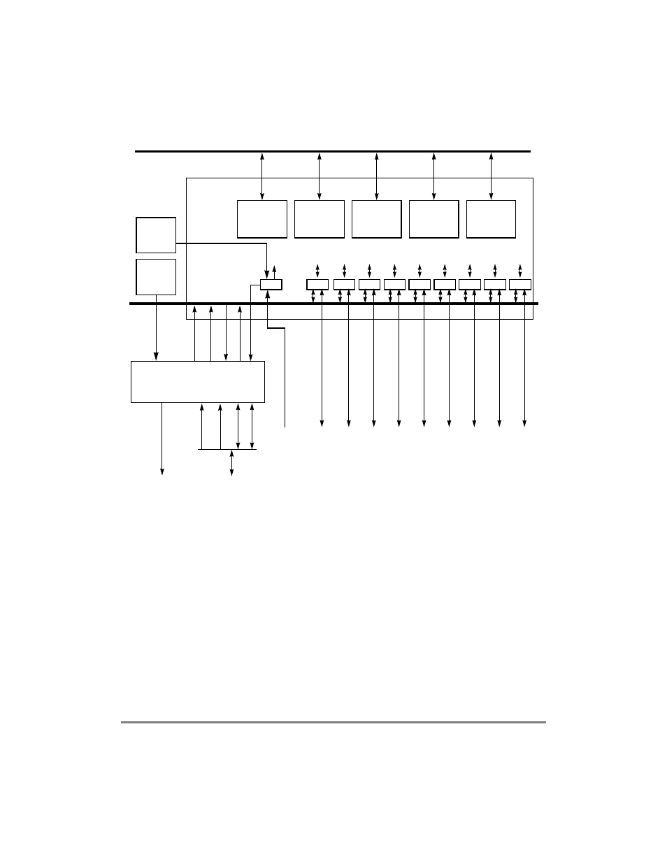
Figure 15-1. CPM Multiplexing Logic (CMX) Block Diagram
15.1 Features
The NMSI mode supports the following:
¥
Each FCC, SCC, and SMC can be programmed independently to work with a serial
deviceÕs own set of pins in a non-multiplexed manner.
¥
Each FCC can be connected to its own MII (media-independent interface).
¥
FCC1 can also be connected to an 8- or 16-bit ATM UTOPIA level-2 interface.
¥
FCC2 can also be connected also to an 8-bit ATM UTOPIA level-2 interface.
¥
Each SCC can have its own set of modem control pins.
¥
Each SMC can have its own set of four pins.
¥
Each FCC, SCC, and SMC can be driven from a bank of twenty clock pins or a bank
of eight BRGs.
Time-Slot Assigner
SIx
R clocks
T clocks
R sync
T sync
TDM Ax, Bx, Cx, Dx
Pins
Strobes
Register Bus
TDM Ax, Bx, Cx, Dx
Tx
TX
SMC1
Nonmultiplexed Serial Interface (NMSI) Pins
Rx
Rx
Clocks
CPM Mux
BRGs
To Serials:
UTOPIA
Address
Register
(CMXUAR)
SMC
Clock
Register
(CMXSMR)
SCC
Clock
Register
(CMXSCR)
FCC
Clock
Register
(CMXFCR)
SIx
Clock
Registers
(CMXSIxCR)
SMC1
MCCs
MUX
MII3
FCC3
MUX
MII2/
FCC2
MUX
MII1/
FCC1
MUX
SCC4
SCC4
MUX
SCC3
SCC3
MUX
SCC2
SCC2
MUX
SCC1
SCC1
MUX
SMC2
SMC2
MUX
UTOPIA
8/16
UTOPIA
8
MUX
