1 the general scc mode registers (gsmr1–gsmr4), The general scc mode registers (gsmr1ðgsmr4) -3, Gsmr_hñgeneral scc mode register (high order) -3 – Motorola MPC8260 User Manual
Page 559: 1 the general scc mode registers (gsmr1ðgsmr4)

MOTOROLA
Chapter 19. Serial Communications Controllers (SCCs)
19-3
Part IV. Communications Processor Module
¥
DPLL circuitry for clock recovery with NRZ, NRZI, FM0, FM1, Manchester, and
Differential Manchester (also known as Differential Bi-phase-L)
¥
Clocks can be derived from a baud rate generator, an external pin, or DPLL
¥
Data rate for asynchronous communication can be as high as 16.62 Mbps at
133 MHz
¥
Supports automatic control of the RTS, CTS, and CD modem signals
¥
Multi-buffer data structure for receive and send (the number of buffer descriptors
(BDs) is limited only by the size of the internal dual-port RAMÑ8 bytes per BD)
¥
Deep FIFOs (SCC send and receive FIFOs are 32 bytes each.)
¥
Transmit-on-demand feature decreases time to frame transmission (transmit
latency)
¥
Low FIFO latency option for send and receive in character-oriented and totally
transparent protocols
¥
Frame preamble options
¥
Full-duplex operation
¥
Fully transparent option for one half of an SCC (Rx/Tx) while another protocol
executes on the other half (Tx/Rx)
¥
Echo and local loopback modes for testing
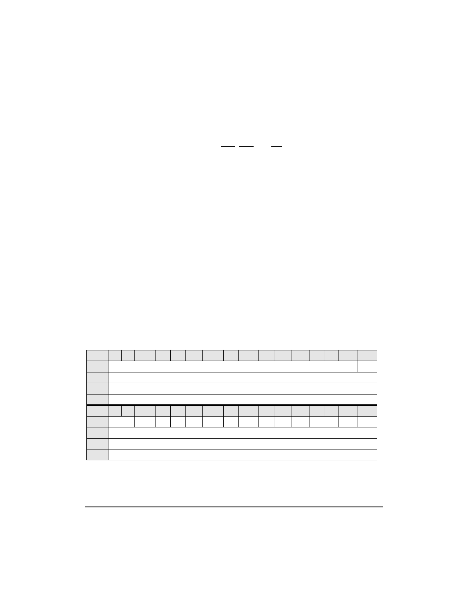
19.1.1 The General SCC Mode Registers (GSMR1ÐGSMR4)
Each SCC contains a general SCC mode register (GSMR) that deÞnes options common to
each SCC regardless of the protocol. GSMR_L contains the low-order 32 bits; GSMR_H,
shown in Figure 19-2, contains the high-order 32 bits. Some GSMR operations are
described in later sections.
Bit
0
1
2
3
4
5
6
7
8
9
10
11
12
13
14
15
Field
Ñ
GDE
Reset
0000_0000_0000_0000
R/W
R/W
Addr
0x11A04 (GSMR1); 0x11A24 (GSMR2); 0x11A44 (GSMR3); 0x11A64 (GSMR4)
Bit
16
17
18
19
20
21
22
23
24
25
26
27
28
29
30
31
Field
TCRC
REVD TRX TTX CDP
CTSP CDS CTSS
TFL
RFW TXSY
SYNL
RTSM RSYN
Reset
0000_0000_0000_0000
R/W
R/W
Addr
0x11A06 (GSMR1); 0x11A26 (GSMR2); 0x11A46 (GSMR3); 0x11A66 (GSMR4)
Figure 19-2. GSMR_HÑGeneral SCC Mode Register (High Order)
