3 external clock inputs, 4 main pll, 1 pll block diagram – Motorola MPC8260 User Manual
Page 271: External clock inputs -5, Main pll -5, Pll block diagram -5, System pll block diagram -5
MOTOROLA
Chapter 9. Clocks and Power Control
9-5
Part III. The Hardware Interface
9.3 External Clock Inputs
The input clock source to the PLL is an external clock oscillator at the bus frequency. The
PLL skew elimination between the CLOCKIN pin and the internal bus clock is guaranteed.
9.4 Main PLL
The main PLL performs frequency multiplication and skew elimination. It allows the
processor to operate at a high internal clock frequency using a low-frequency clock input,
which has two immediate beneÞts: A lower clock input frequency reduces overall
electromagnetic interference generated by the system, and oscillating at different
frequencies eliminates the need for another oscillator to the system.
9.4.1 PLL Block Diagram
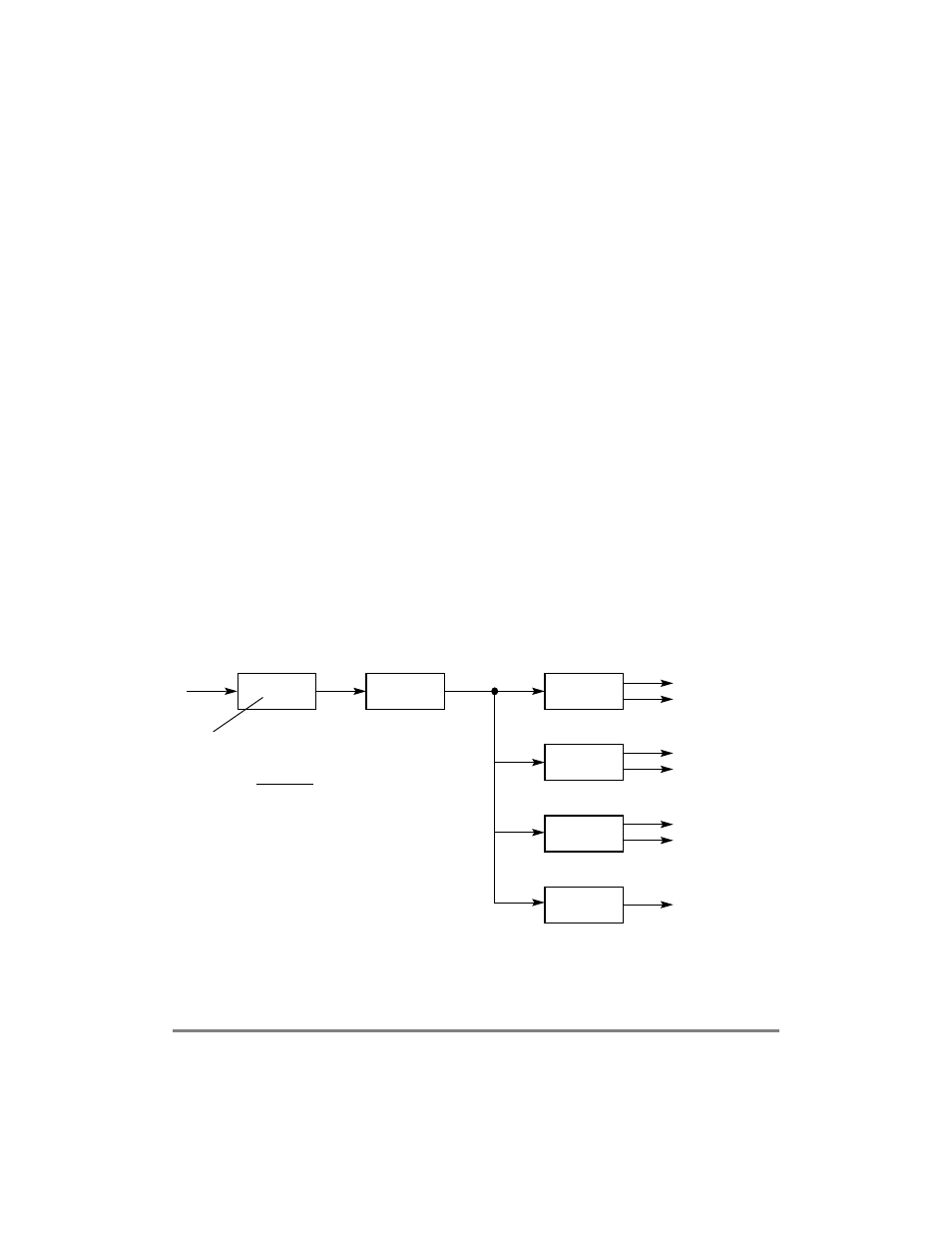
Figure 9-1 shows how clocking is implemented and the interdependencies of the SCMR
Þelds:
¥
BUSDFÑ60x bus division factor
¥
CPMDFÑCPM division factor. This value is always 1.
¥
PLLDFÑPLL pre-divider value. Ensures that PLLMF is an integer value regardless
of whether CPM_CLK/CLKIN is an integer.
¥
PLLMFÑPLL multiplication factor
These Þelds are described in detail in Table 9-5.
Figure 9-1. System PLL Block Diagram
The reference signal (CLKIN) goes to the phase comparator that controls the direction (up
or down) that the charge pump drives the voltage across the external Þlter capacitor (XFC).
÷ (PLLDF + 1)
VCO_OUT
´
2
(PLLMF + 1)
÷ (CPMDF + 1)
÷ (BUSDF + 1)
÷ 4
2
2 (DFBRG + 1)
CPM_CLK
CPM_CLK_90°
BUS_CLK (= CLKIN)
BUS_CLK_90°
SCC_CLK
SCC_CLK_90°
BRG
CLKIN
(÷2)
PLLDF ensures that PLLMF is an integer, according to the
following formula:
PLLMF =
CPM_CLK
CLKIN
´
(PLLDF + 1) Ð 1
General-Purpose Divider
(2*CPM_CLK)