1 32-bit wide memory bank connection, Section 5–11.1, Nxp semiconductors – NXP Semiconductors LPC24XX UM10237 User Manual
Page 97
UM10237_4
© NXP B.V. 2009. All rights reserved.
User manual
Rev. 04 — 26 August 2009
97 of 792
NXP Semiconductors
UM10237
Chapter 5: LPC24XX External Memory Controller (EMC)
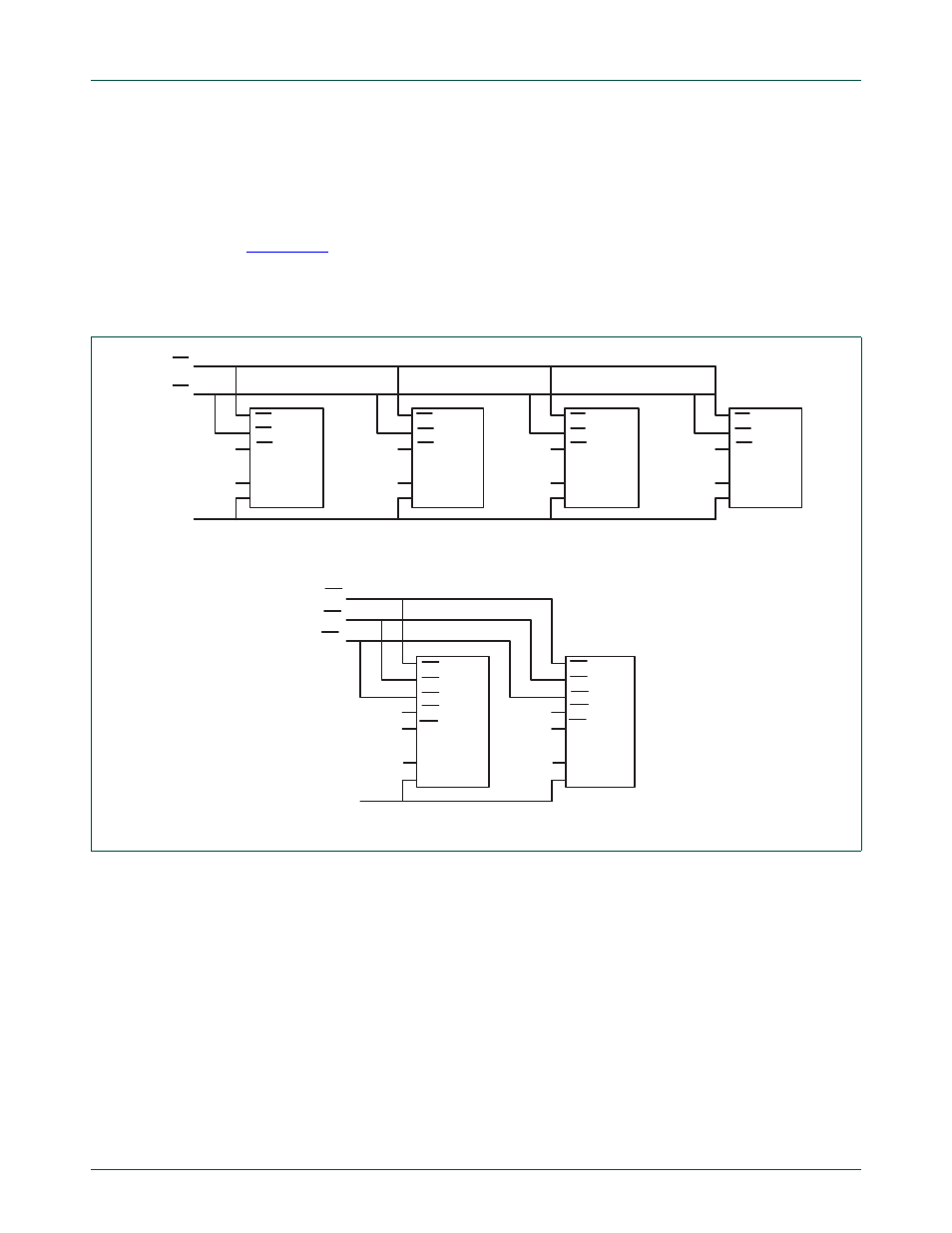
Symbol "a_b" in the following figures refers to the highest order address line in the data
bus. Symbol "a_m" refers to the highest order address line of the memory chip used in the
external memory interface.
If the external memory is used as external boot memory for flashless devices, refer to
on how to connect the EMC. The memory bank width for memory banks 1
and 2 is determined by the setting of the two BOOT1/0 pins.
11.1 32-bit wide memory bank connection
a. 32 bit wide memory bank interfaced to four 8 bit memory chips
b. 32 bit wide memory bank interfaced to two 16 bit memory chips
A[a_b:2]
BLS[1]
D[15:8]
CE
OE
WE
IO[7:0]
A[a_m:0]
BLS[0]
D[7:0]
CE
OE
WE
IO[7:0]
A[a_m:0]
OE
CS
BLS[3]
D[31:24]
CE
OE
WE
IO[7:0]
A[a_m:0]
BLS[2]
D[23:16]
CE
OE
WE
IO[7:0]
A[a_m:0]
OE
CS
WE
CE
OE
WE
UB
LB
IO[15:0]
A[a_m:0]
D[31:16]
BLS[2]
CE
OE
WE
UB
LB
IO[15:0]
A[a_m:0]
D[15:0]
BLS[0]
A[a_b:2]
BLS[3]
BLS[1]