Register description, Figure 20–102, Nxp semiconductors – NXP Semiconductors LPC24XX UM10237 User Manual
Page 544
UM10237_4
© NXP B.V. 2009. All rights reserved.
User manual
Rev. 04 — 26 August 2009
544 of 792
NXP Semiconductors
UM10237
Chapter 20: LPC24XX SSP interface SSP0/1
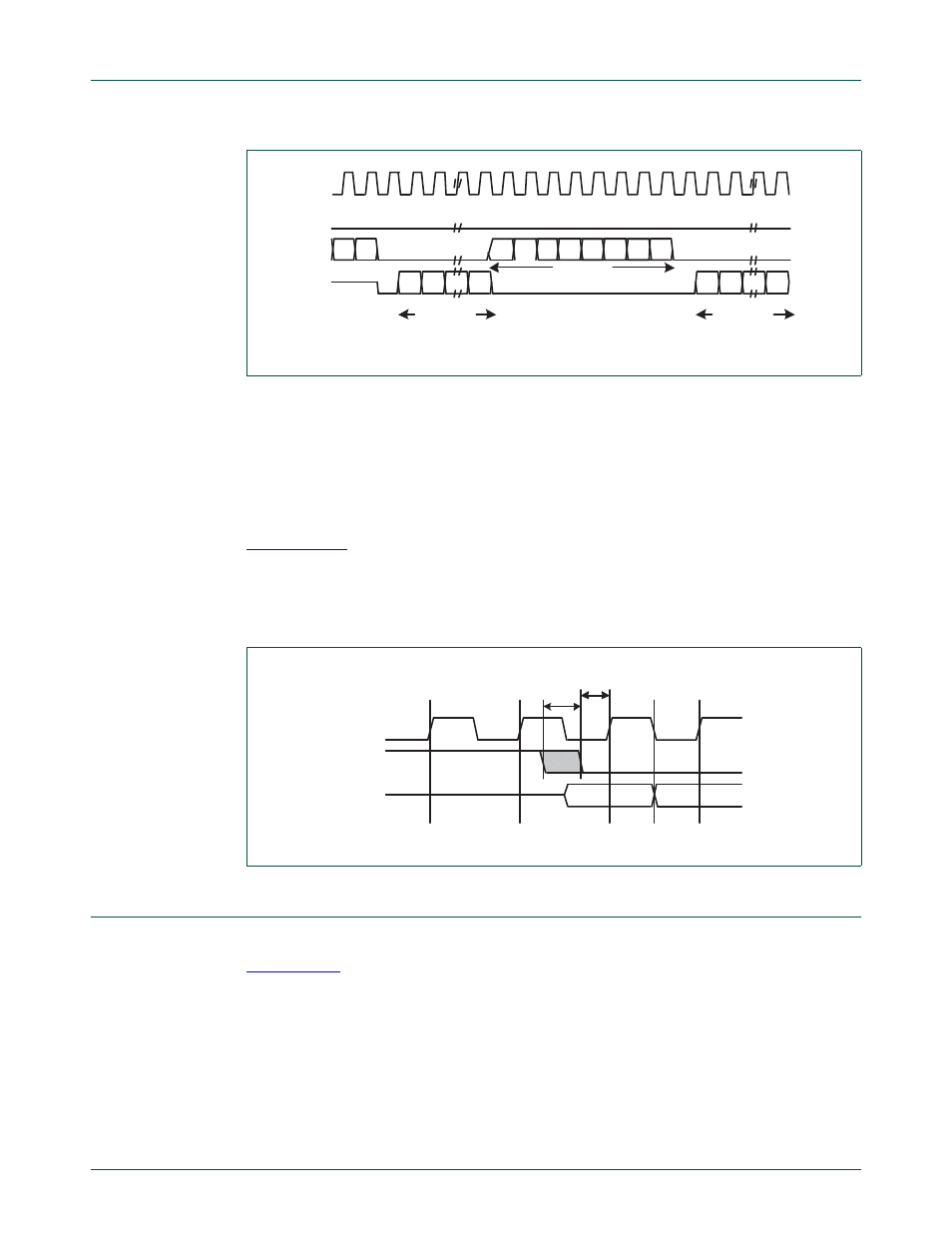
5.3.1 Setup and hold time requirements on CS with respect to SK in Microwire
mode
In the Microwire mode, the SSP slave samples the first bit of receive data on the rising
edge of SK after CS has gone LOW. Masters that drive a free-running SK must ensure
that the CS signal has sufficient setup and hold margins with respect to the rising edge of
SK.
illustrates these setup and hold time requirements. With respect to the SK
rising edge on which the first bit of receive data is to be sampled by the SSP slave, CS
must have a setup of at least two times the period of SK on which the SSP operates. With
respect to the SK rising edge previous to this edge, CS must have a hold of at least one
SK period.
6.
Register description
The register offsets from the SSP controller base addresses are shown in the
Fig 102. Microwire frame format (continuos transfers)
SK
CS
SO
SI
MSB
LSB
4 to 16 bits
output data
8 bit control
4 to 16 bits
output data
MSB
LSB
0
MSB
LSB
LSB
Fig 103. Microwire frame format setup and hold details
SK
CS
SI
t
HOLD
= t
SK
t
SETUP
=2*t
SK