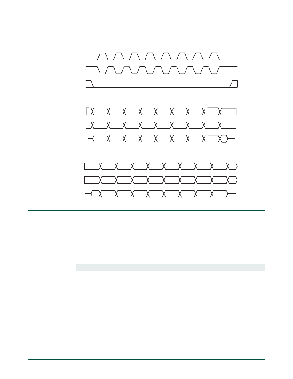
Figure 19–94, Nxp semiconductors – NXP Semiconductors LPC24XX UM10237 User Manual
Page 527
UM10237_4
© NXP B.V. 2009. All rights reserved.
User manual
Rev. 04 — 26 August 2009
527 of 792
NXP Semiconductors
UM10237
Chapter 19: LPC24XX SPI
The data and clock phase relationships are summarized in
. This table
summarizes the following for each setting of CPOL and CPHA.
•
When the first data bit is driven.
•
When all other data bits are driven.
•
When data is sampled.
The definition of when an 8 bit transfer starts and stops is dependent on whether a device
is a master or a slave, and the setting of the CPHA variable.
When a device is a master, the start of a transfer is indicated by the master having a byte
of data that is ready to be transmitted. At this point, the master can activate the clock, and
begin the transfer. The transfer ends when the last clock cycle of the transfer is complete.
Fig 94. SPI data transfer format (CPHA = 0 and CPHA = 1)
MISO (CPHA = 1)
MOSI (CPHA = 1)
Cycle # CPHA = 1
CPHA = 1
MISO (CPHA = 0)
MOSI (CPHA = 0)
Cycle # CPHA = 0
CPHA = 0
SSEL
SCK (CPOL = 1)
SCK (CPOL = 0)
1
2
3
8
7
6
5
4
BIT 1
BIT 2
BIT 3
BIT 8
BIT 7
BIT 6
BIT 5
BIT 4
BIT 1
BIT 2
BIT 3
BIT 8
BIT 7
BIT 6
BIT 5
BIT 4
1
2
3
8
7
6
5
4
BIT 1
BIT 2
BIT 3
BIT 8
BIT 7
BIT 6
BIT 5
BIT 4
BIT 1
BIT 2
BIT 3
BIT 8
BIT 7
BIT 6
BIT 5
BIT 4
Table 459. SPI Data To Clock Phase Relationship
CPOL and CPHA settings First data driven
Other data driven
Data sampled
CPOL = 0, CPHA = 0
Prior to first SCK rising edge SCK falling edge
SCK rising edge
CPOL = 0, CPHA = 1
First SCK rising edge
SCK rising edge
SCK falling edge
CPOL = 1, CPHA = 0
Prior to first SCK falling edge SCK rising edge
SCK falling edge
CPOL = 1, CPHA = 1
First SCK falling edge
SCK falling edge
SCK rising edge