1 analog transceiver, 2 serial interface engine (sie), 3 endpoint ram (ep_ram) – NXP Semiconductors LPC24XX UM10237 User Manual
Page 332: 4 ep_ram access control, Nxp semiconductors
UM10237_4
© NXP B.V. 2009. All rights reserved.
User manual
Rev. 04 — 26 August 2009
332 of 792
NXP Semiconductors
UM10237
Chapter 13: LPC24XX USB device controller
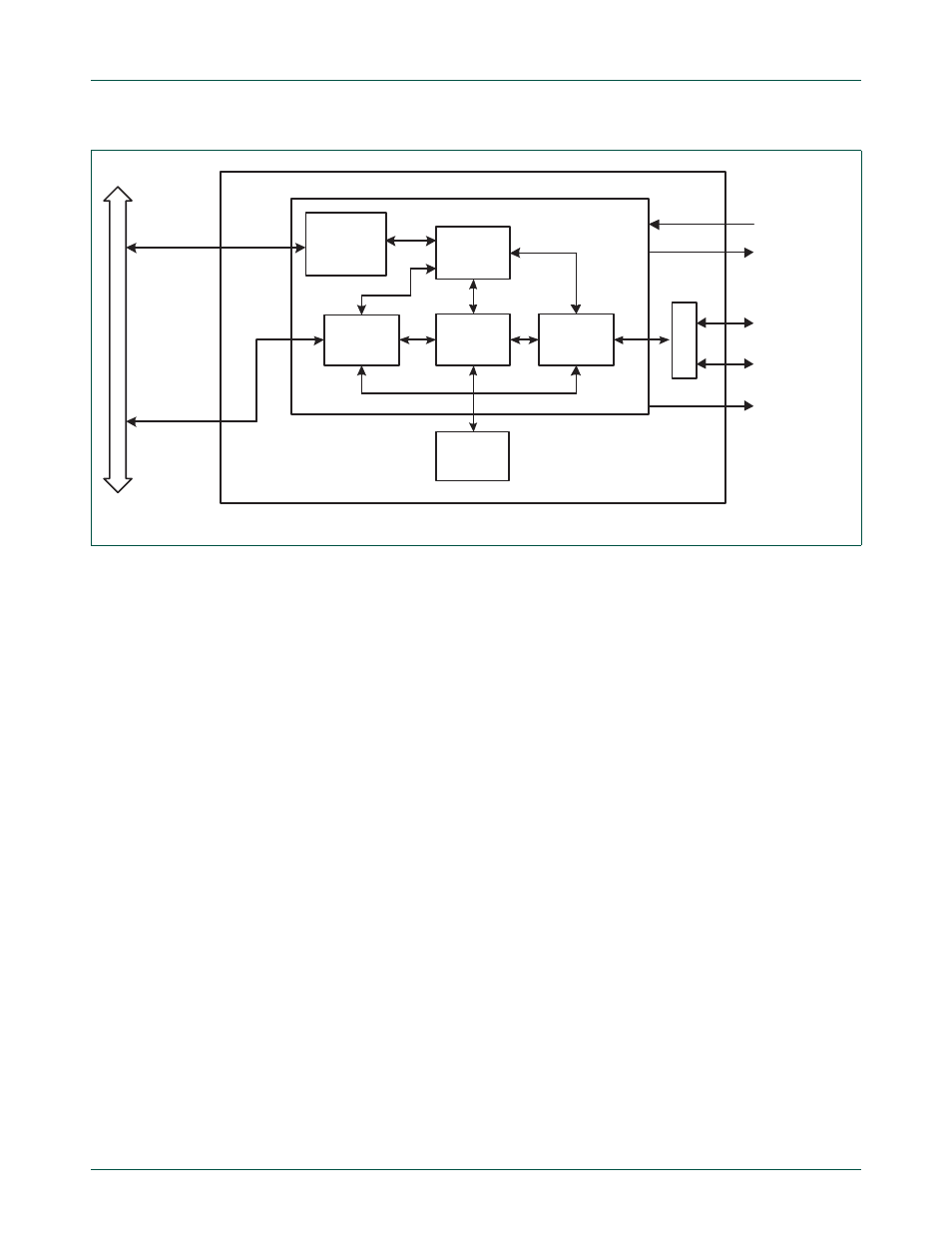
5.1 Analog transceiver
The USB Device Controller has a built-in analog transceiver (ATX). The USB ATX
sends/receives the bi-directional D+ and D- signals of the USB bus.
5.2 Serial Interface Engine (SIE)
The SIE implements the full USB protocol layer. It is completely hardwired for speed and
needs no firmware intervention. It handles transfer of data between the endpoint buffers in
EP_RAM and the USB bus. The functions of this block include: synchronization pattern
recognition, parallel/serial conversion, bit stuffing/de-stuffing, CRC checking/generation,
PID verification/generation, address recognition, and handshake evaluation/generation.
5.3 Endpoint RAM (EP_RAM)
Each endpoint buffer is implemented as an SRAM based FIFO. The SRAM dedicated for
this purpose is called the EP_RAM. Each realized endpoint has a reserved space in the
EP_RAM. The total EP_RAM space required depends on the number of realized
endpoints, the maximum packet size of the endpoint, and whether the endpoint supports
double buffering.
5.4 EP_RAM access control
The EP_RAM Access Control logic handles transfer of data from/to the EP_RAM and the
three sources that can access it: the CPU (via the Register Interface), the SIE, and the
DMA Engine.
Fig 45. USB device controller block diagram
register
interface
(AHB slave)
DMA interface
(AHB master)
EP_RAM
(4K)
EP_RAM
ACCESS
CONTROL
REGISTER
INTERFACE
SERIAL
INTERFACE
ENGINE
DMA
ENGINE
USB DEVICE
BLOCK
U
SB AT
X
BUS
MASTER
INTERFACE
AH
B BU
S
V
BUS
USB_CONNECT1,
USB_CONNECT2
USB_D+1,
USB_D+2
USB_D-1,
USB_D-2
USB_UP_LED1,
USB_UP_LED2