Own in, Figure 22–111, Nxp semiconductors – NXP Semiconductors LPC24XX UM10237 User Manual
Page 573
UM10237_4
© NXP B.V. 2009. All rights reserved.
User manual
Rev. 04 — 26 August 2009
573 of 792
NXP Semiconductors
UM10237
Chapter 22: LPC24XX I
2
C interfaces I
2
C0/1/2
•
Data transfer from a slave transmitter to a master receiver. The first byte (the slave
address) is transmitted by the master. The slave then returns an acknowledge bit.
Next follows the data bytes transmitted by the slave to the master. The master returns
an acknowledge bit after all received bytes other than the last byte. At the end of the
last received byte, a “not acknowledge” is returned. The master device generates all
of the serial clock pulses and the START and STOP conditions. A transfer is ended
with a STOP condition or with a repeated START condition. Since a repeated START
condition is also the beginning of the next serial transfer, the I
2
C bus will not be
released.
Each of the three I
2
C interfaces on the LPC2400 is byte oriented, and has four operating
modes: master transmitter mode, master receiver mode, slave transmitter mode and
slave receiver mode.
The three I
2
C interfaces are identical except for the pin I/O characteristics. I
2
C0 complies
with entire I
2
C specification, supporting the ability to turn power off to the LPC2400
without causing a problem with other devices on the same I
2
C bus (see "The I
2
C-bus
specification" description under the heading "Fast-Mode", and notes for the table titled
"Characteristics of the SDA and SCL I/O stages for F/S-mode I
2
C-bus devices"). This is
sometimes a useful capability, but intrinsically limits alternate uses for the same pins if the
I2C interface is not used. Seldom is this capability needed on multiple I2C interfaces
within the same microcontroller. Therefore, I
2
C1 and I
2
C2 are implemented using
standard port pins, and do not support the ability to turn power off to the LPC2400 while
leaving the I
2
C bus functioning between other devices. This difference should be
considered during system design while assigning uses for the I
2
C interfaces.
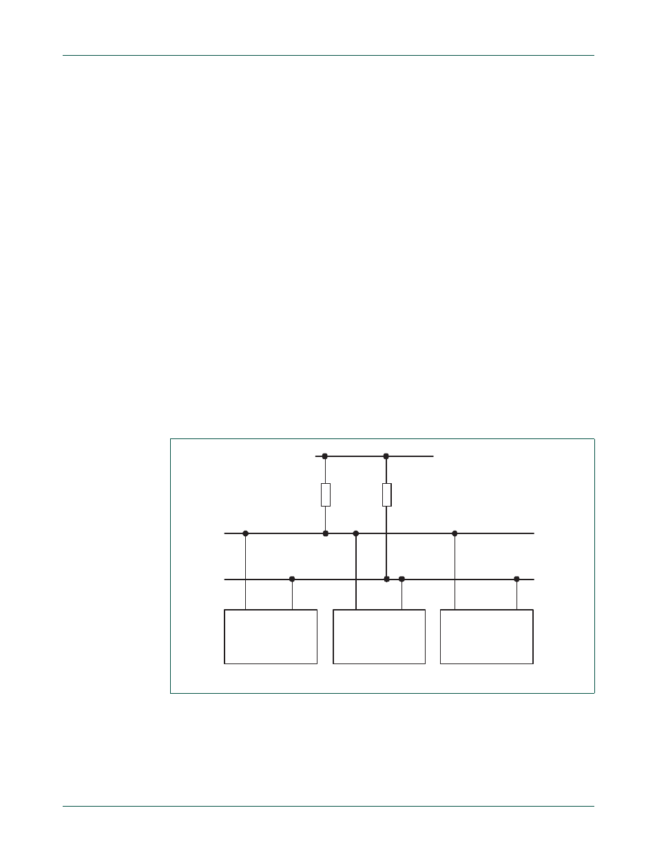
Fig 111. I
2
C bus configuration
OTHER DEVICE WITH
I
2
C INTERFACE
pull-up
resistor
OTHER DEVICE WITH
I
2
C INTERFACE
LPC2400
SDA
SCL
I
2
C bus
SCL
SDA
pull-up
resistor