Nxp semiconductors, 1 pll operation – NXP Semiconductors LPC24XX UM10237 User Manual
Page 47
UM10237_4
© NXP B.V. 2009. All rights reserved.
User manual
Rev. 04 — 26 August 2009
47 of 792
NXP Semiconductors
UM10237
Chapter 4: LPC24XX Clocking and power control
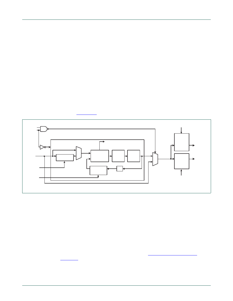
3.2.1 PLL operation
The PLL input, in the range of 32 kHZ to 24 MHz, may initially be divided down by a value
"N", which may be in the range of 1 to 256. This input division provides a greater number
of possibilities in providing a wide range of output frequencies from the same input
frequency.
Following the PLL input divider is the PLL multiplier. The multiplier can multiply the input
divider output through the use of a Current Controlled Oscillator (CCO) by a value "M", in
the range of 1 through 32768. The resulting frequency must be in the range of 275 MHz to
550 MHz. The multiplier works by dividing the CCO output by the value of M, then using a
phase-frequency detector to compare the divided CCO output to the multiplier input. The
error value is used to adjust the CCO frequency.
There are additional dividers at the PLL output to bring the frequency down to what is
needed for the CPU, USB, and other peripherals. The PLL output dividers are described
in the Clock Dividers section following the PLL description. A block diagram of the PLL is
shown in
PLL activation is controlled via the PLLCON register. The PLL multiplier and divider
values are controlled by the PLLCFG register. These two registers are protected in order
to prevent accidental alteration of PLL parameters or deactivation of the PLL. Since all
chip operations, including the Watchdog Timer, could be dependent on the PLL if so
configured (for example when it is providing the chip clock), accidental changes to the PLL
setup could result in unexpected or fatal behavior of the microcontroller. The protection is
accomplished by a feed sequence similar to that of the Watchdog Timer. Details are
provided in the description of the PLLFEED register.
The PLL is turned off and bypassed following a chip Reset and by entering Power-down
mode. PLL is enabled by software only.
It is important that the setup procedure described in
is followed as is or the PLL might not operate at all!.
Fig 14. PLL block diagram (N = 16, M = 125, USBSEL = 6, CCLKSEL = 4)
N-DIVIDER
M-DIVIDER
PHASE-
FREQUENCY
DETECTOR
FILTER
CCO
/2
CPU
CLOCK
DIVIDER
cclk =
72 MHz
CCLKSEL[7:0]
PLOCK
PLLE
PLLC
pd
USB
CLOCK
DIVIDER
usbclk =
48 MHz
USBSEL[3:0]
refclk =
1.152 MHz
pllclkin =
18.432 MHz
pllclk =
288 MHz
/16
/125
1.152 MHz
144 MHz
288 MHz
288
MHz
/6
/4
NSEL[23:16]
MSEL[14:0]