Nxp semiconductors – NXP Semiconductors LPC24XX UM10237 User Manual
Page 153
UM10237_4
© NXP B.V. 2009. All rights reserved.
User manual
Rev. 04 — 26 August 2009
153 of 792
NXP Semiconductors
UM10237
Chapter 8: LPC24XX Pin configuration
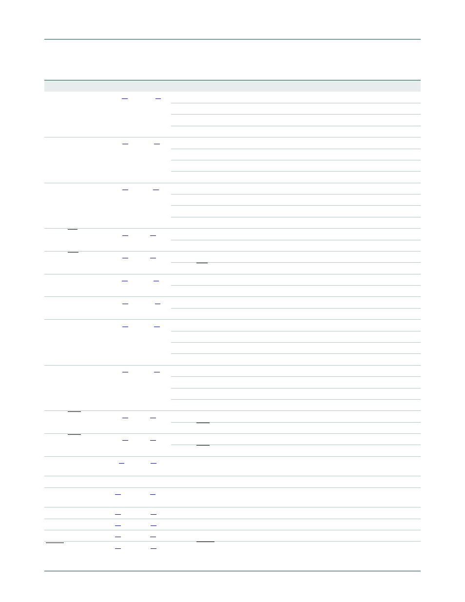
P4[21]/A21/
SCL2/SSEL1
115
M15
I/O
P4[21] — General purpose digital input/output pin.
I/O
A21 — External memory address line 21.
I/O
SCL2 — I
2
C2 clock input/output (this is not an open-drain pin).
I/O
SSEL1 — Slave Select for SSP1.
P4[22]/A22/
TXD2/MISO1
I/O
P4[22] — General purpose digital input/output pin.
I/O
A22 — External memory address line 22.
O
TXD2 — Transmitter output for UART2.
I/O
MISO1 — Master In Slave Out for SSP1.
P4[23]/A23/
RXD2/MOSI1
J15
I/O
P4[23] — General purpose digital input/output pin.
I/O
A23 — External memory address line 23.
I
RXD2 — Receiver input for UART2.
I/O
MOSI1 — Master Out Slave In for SSP1.
P4[24]/OE
I/O
P4[24] — General purpose digital input/output pin.
O
OE — LOW active Output Enable signal.
P4[25]/WE
I/O
P4[25] — General purpose digital input/output pin.
O
WE — LOW active Write Enable signal.
P4[26]/BLS0
119
L15
I/O
P4[26] — General purpose digital input/output pin.
O
BLS0 — LOW active Byte Lane select signal 0.
P4[27]/BLS1
G15
I/O
P4[27] — General purpose digital input/output pin.
O
BLS1 — LOW active Byte Lane select signal 1.
P4[28]/BLS2/
MAT2[0]/TXD3
C11
I/O
P4 [28] — General purpose digital input/output pin.
O
BLS2 — LOW active Byte Lane select signal 2.
O
MAT2[0] — Match output for Timer 2, channel 0.
O
TXD3 — Transmitter output for UART3.
P4[29]/BLS3/
MAT2[1]/RXD3
I/O
P4[29] — General purpose digital input/output pin.
O
BLS3 — LOW active Byte Lane select signal 3.
O
MAT2[1] — Match output for Timer 2, channel 1.
I
RXD3 — Receiver input for UART3.
P4[30]/CS0
I/O
P4[30] — General purpose digital input/output pin.
O
CS0 — LOW active Chip Select 0 signal.
P4[31]/CS1
I/O
P4[31] — General purpose digital input/output pin.
O
CS1 — LOW active Chip Select 1 signal.
ALARM
37
O
ALARM — RTC controlled output. This is a 1.8 V pin. It goes HIGH when
a RTC alarm is generated.
USB_D
−2
52
U1
I/O
USB_D
−2 — USB port 2 bidirectional D− line.
DBGEN
9
F4
I
DBGEN — JTAG interface control signal. Also used for boundary
scanning.
TDO
2
O
TDO — Test data out for JTAG interface.
TDI
4
I
TDI — Test data in for JTAG interface.
TMS
6
I
TMS — Test Mode Select for JTAG interface.
TRST
8
I
TRST — Test Reset for JTAG interface.
Table 122. LPC2420/60/68 pin description
…continued
Symbol
Pin
Ball
Type
Description