Table 9–143, Lcd fu, Nxp semiconductors – NXP Semiconductors LPC24XX UM10237 User Manual
Page 189
UM10237_4
© NXP B.V. 2009. All rights reserved.
User manual
Rev. 04 — 26 August 2009
189 of 792
NXP Semiconductors
UM10237
Chapter 9: LPC24XX Pin connect
5.11 Pin Function Select Register 10 (PINSEL10 - 0xE002 C028)
Only bit 3 of this register is used to control the ETM interface pins.
The value of the RTCK I/O pin is sampled when the external reset is asserted. When
RTCK pin is low during external reset, bit 3 in PINSEL10 is set to enable the ETM
interface pins. When RTCK pin is high during external reset, bit 3 in PINSEL10 is cleared
to disable the ETM interface pins.
The ETM interface control pin can also be modified by the software.
21:20
P4[26]
GPIO Port 4.26
BLS0
Reserved
Reserved
00
23:22
P4[27]
GPIO Port 4.27
BLS1
Reserved
Reserved
00
25:24
P4[28]
GPIO Port 4.28
Reserved
MAT2[0]
TXD3
00
27:26
P4[29]
GPIO Port 4.29
Reserved
MAT2[1]
RXD3
00
29:28
P4[30]
GPIO Port 4.30
CS0
Reserved
Reserved
00
31:30
P4[31]
GPIO Port 4.31
CS1
Reserved
Reserved
00
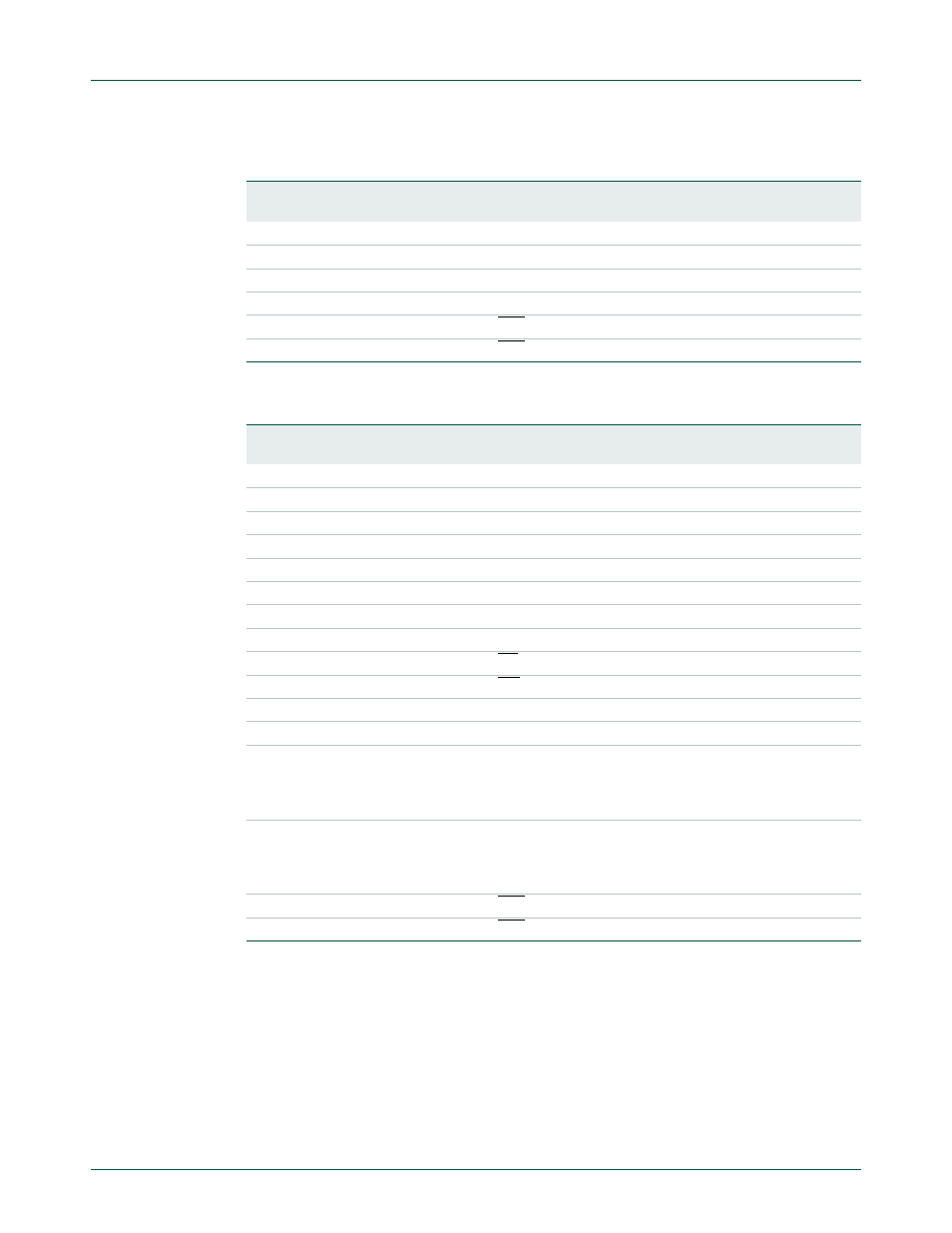
Table 143. LPC2420/60/68/70/78 pin function select register 9 (PINSEL9 - address
0xE002 C024) bit description
PINSEL9 Pin
name
Function when
00
Function
when 01
Function
when 10
Function
when 11
Reset
value
1:0
P4[16]
GPIO Port 4.16
A16
Reserved
Reserved
00
3:2
P4[17]
GPIO Port 4.17
A17
Reserved
Reserved
00
5:4
P4[18]
GPIO Port 4.18
A18
Reserved
Reserved
00
7:6
P4[19]
GPIO Port 4.19
A19
Reserved
Reserved
00
9:8
P4[20]
GPIO Port 4.20
A20
SDA2
SCK1
00
11:10
P4[21]
GPIO Port 4.21
A21
SCL2
SSEL1
00
13:12
P4[22]
GPIO Port 4.22
A22
TXD2
MISO1
00
15:14
P4[23]
GPIO Port 4.23
A23
RXD2
MOSI1
00
17:16
P4[24]
GPIO Port 4.24
OE
Reserved
Reserved
00
19:18
P4[25]
GPIO Port 4.25
WE
Reserved
Reserved
00
21:20
P4[26]
GPIO Port 4.26
BLS0
Reserved
Reserved
00
23:22
P4[27]
GPIO Port 4.27
BLS1
Reserved
Reserved
00
25:24
P4[28]
GPIO Port 4.28
BLS2
MAT2[0]/
LCDVD[6]/
LCDVD[10]/
LCDVD[2]
TXD3
00
27:26
P4[29]
GPIO Port 4.29
BLS3
MAT2[1]/
LCDVD[7]/
LCDVD[11]/
LCDVD[3]
RXD3
00
29:28
P4[30]
GPIO Port 4.30
CS0
Reserved
Reserved
00
31:30
P4[31]
GPIO Port 4.31
CS1
Reserved
Reserved
00
Table 142. LPC2458 pin function select register 9 (PINSEL9 - address 0xE002 C024) bit
description
PINSEL9 Pin
name
Function when
00
Function
when 01
Function
when 10
Function
when 11
Reset
value