7 otg timer register (otgtmr - 0xffe0 c114), Section, 15–7.7 “otg timer register (otgtmr - 0xffe0 c114) – NXP Semiconductors LPC24XX UM10237 User Manual
Page 404: The tmr bit is, Nxp semiconductors
UM10237_4
© NXP B.V. 2009. All rights reserved.
User manual
Rev. 04 — 26 August 2009
404 of 792
NXP Semiconductors
UM10237
Chapter 15: LPC24XX USB OTG controller
7.7 OTG Timer Register (OTGTmr - 0xFFE0 C114)
7.8 OTG Clock Control Register (OTGClkCtrl - 0xFFE0 CFF4)
This register controls the clocking of the OTG controller. Whenever software wants to
access the registers, the corresponding clock control bit needs to be set. The software
does not have to repeat this exercise for every register access, provided that the
corresponding OTGClkCtrl bits are already set.
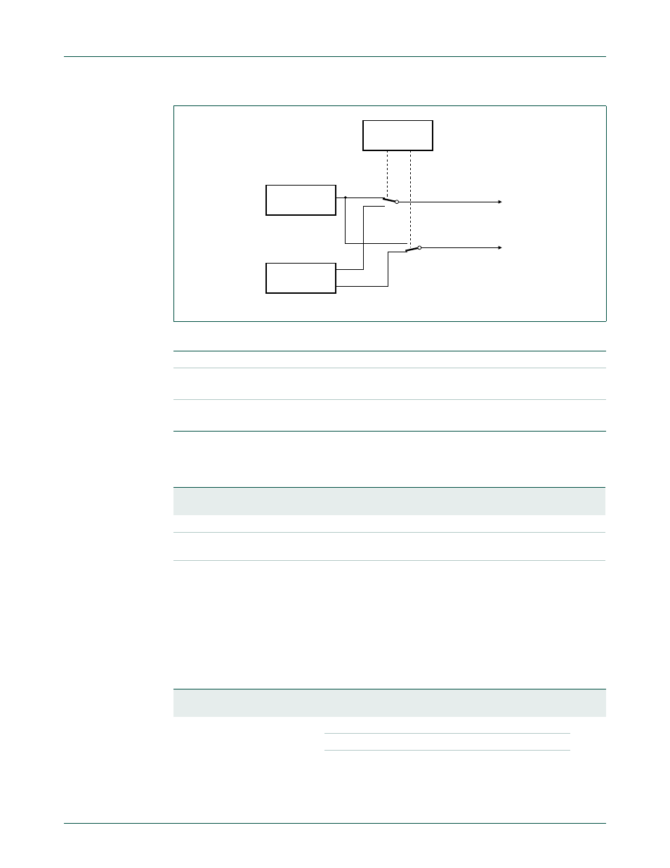
Fig 57. Port selection for PORT_FUNC bit 0 = 0 and PORT_FUNC bit 1 = 0.
Table 366. Port function truth table
PORT_FUNC[0] = 0
PORT_FUNC[0] = 1
PORT_FUNC[1] = 0
U1 = device (OTG)
U2 = host
U1 = host (OTG)
U2 = host
PORT_FUNC[1] = 1
reserved
U1 = host
U2 = device
DEVICE
CONTROLLER
HOST
CONTROLLER
OTGStCtrl
PORT_FUNC[1] = 0
PORT_FUNC[0] = 0
U1
U2
port2
port1
port1
Table 367. OTG Timer register (OTGTmr - address 0xFFE0 C114) bit description
Bit
Symbol
Description
Reset
Value
15:0
TIMEOUT_CNT The TMR interrupt is set when TMR_CNT reaches this value.
0xFFFF
31:16 -
Reserved, user software should not write ones to reserved
bits. The value read from a reserved bit is not defined.
NA
Table 368. OTG_clock_control register (OTG_clock_control - address 0xFFE0 CFF4) bit
description
Bit
Symbol
Value
Description
Reset
Value
0
HOST_CLK_EN
Host clock enable
0
0
Disable the Host clock.
1
Enable the Host clock.