Figure 2–8, Nxp semiconductors – NXP Semiconductors LPC24XX UM10237 User Manual
Page 20
UM10237_4
© NXP B.V. 2009. All rights reserved.
User manual
Rev. 04 — 26 August 2009
20 of 792
NXP Semiconductors
UM10237
Chapter 2: LPC24XX Memory mapping
All peripheral register addresses are word aligned (to 32 bit boundaries) regardless of
their size. This eliminates the need for byte lane mapping hardware that would be required
to allow byte (8 bit) or half-word (16 bit) accesses to occur at smaller boundaries. An
implication of this is that word and half-word registers must be accessed all at once. For
example, it is not possible to read or write the upper byte of a word register separately.
(1) LPC247x only.
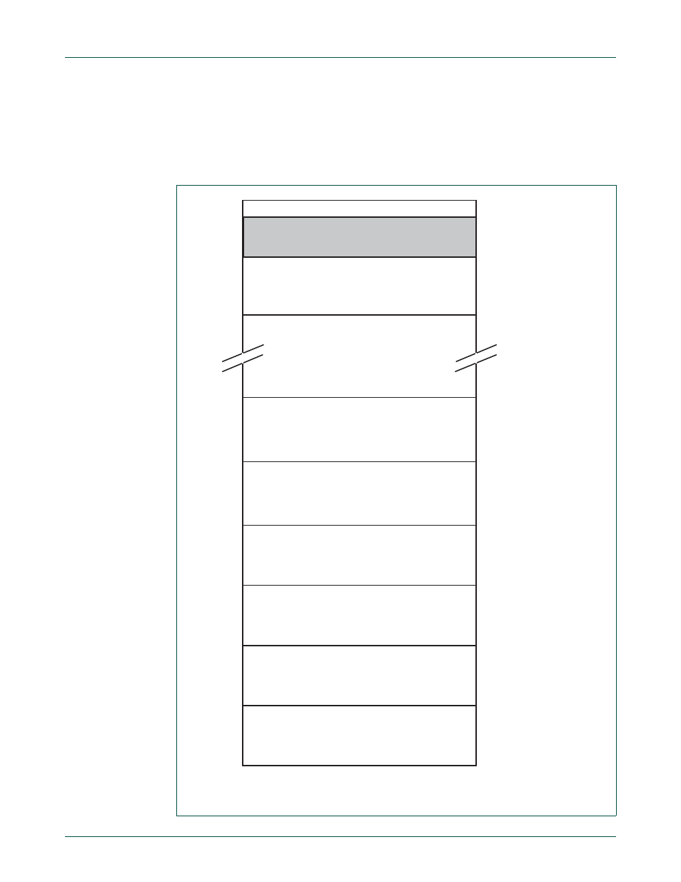
Fig 8.
AHB peripheral map
VECTORED INTERRUPT CONTROLLER
(AHB PERIPHERAL #0)
0xFFFF F000 (4G - 4K)
0xFFFF C000
0xFFFF 8000
(AHB PERIPHERAL #4)
(AHB PERIPHERAL #3)
(AHB PERIPHERAL #2)
(AHB PERIPHERAL #1)
(AHB PERIPHERAL #126)
0xFFE1 8000
0xFFE1 4000
0xFFE1 0000
0xFFE0 C000
0xFFE0 8000
0xFFE0 4000
0xFFE0 0000
ETHERNET CONTROLLER
GENERAL PURPOSE DMA CONTROLLER
EXTERNAL MEMORY CONTROLLER
USB CONTROLLER
LCD
(1)
(AHB PERIPHERAL #5)
NOT USED