Register description, Nxp semiconductors – NXP Semiconductors LPC24XX UM10237 User Manual
Page 303
UM10237_4
© NXP B.V. 2009. All rights reserved.
User manual
Rev. 04 — 26 August 2009
303 of 792
NXP Semiconductors
UM10237
Chapter 12: LPC24XX LCD controller
7.
Register description
shows the registers associated with the LCD controller and a summary of
their functions. Following the table are details for each register.
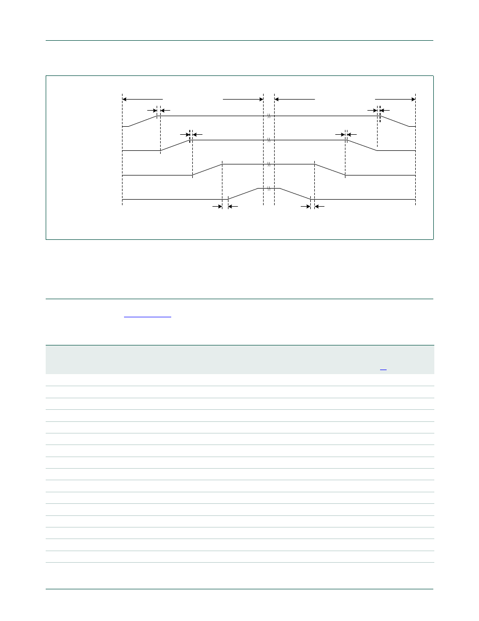
Fig 40. Power-up and power-down sequences
LCDLP, LCDCP,
LCDFP, LCDAC,
LCDLE
LCD Power
Contrast Voltage
LCDPWR,
LCD[23:0]
Minimum 0 ms
LCD on sequence
LCD off sequence
Minimum 0 ms
Minimum 0 ms
Display specific delay
Display specific delay
Minimum 0 ms
Table 259. Summary of LCD controller registers
Address
Name
Description
Reset
value
Access
0xE01F C1B8
LCD_CFG
LCD Configuration and clocking control
0x0
R/W
0xFFE1 0000
LCD_TIMH
Horizontal Timing Control register
0x0
R/W
0xFFE1 0004
LCD_TIMV
Vertical Timing Control register
0x0
R/W
0xFFE1 0008
LCD_POL
Clock and Signal Polarity Control register
0x0
R/W
0xFFE1 000C
LCD_LE
Line End Control register
0x0
R/W
0xFFE1 0010
LCD_UPBASE
Upper Panel Frame Base Address register
0x0
R/W
0xFFE1 0014
LCD_LPBASE
Lower Panel Frame Base Address register
0x0
R/W
0xFFE1 0018
LCD_CTRL
LCD Control register
0x0
R/W
0xFFE1 001C
LCD_INTMSK
Interrupt Mask register
0x0
R/W
0xFFE1 0020
LCD_INTRAW
Raw Interrupt Status register
0x0
RO
0xFFE1 0024
LCD_INTSTAT
Masked Interrupt Status register
0x0
RO
0xFFE1 0028
LCD_INTCLR
Interrupt Clear register
0x0
WO
0xFFE1 002C
LCD_UPCURR
Upper Panel Current Address Value register
0x0
RO
0xFFE1 0030
LCD_LPCURR
Lower Panel Current Address Value register
0x0
RO
0xFFE1 0200 - 0xFFE1 03FC
LCD_PAL
256x16-bit Color Palette registers
0x0
R/W
0xFFE1 0800 - 0xFFE1 0BFC
CRSR_IMG
Cursor Image registers
0x0
R/W
0xFFE1 0C00
CRSR_CTRL
Cursor Control register
0x0
R/W