Mam usage notes, Nxp semiconductors – NXP Semiconductors LPC24XX UM10237 User Manual
Page 107
UM10237_4
© NXP B.V. 2009. All rights reserved.
User manual
Rev. 04 — 26 August 2009
107 of 792
NXP Semiconductors
UM10237
Chapter 6: LPC24XX Memory Accelerator Module (MAM)
8.
MAM usage notes
When changing MAM timing, the MAM must first be turned off by writing a zero to
MAMCR. A new value may then be written to MAMTIM. Finally, the MAM may be turned
on again by writing a value (1 or 2) corresponding to the desired operating mode to
MAMCR.
For a system clock slower than 20 MHz, MAMTIM can be 001. For a system clock
between 20 MHz and 40 MHz, flash access time is suggested to be 2 CCLKs, while in
systems with a system clock faster than 40 MHz, 3 CCLKs are proposed. For system
clocks of 60 MHz and above, 4CCLK’s are needed.
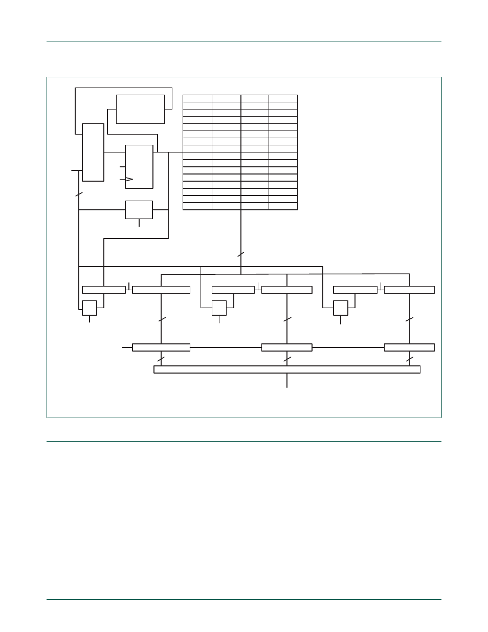
Fig 21. Block diagram of the Memory Accelerator Module
xFFE0
xFFE4
xFFE8
xFFEC
30000
30004
30008
3000C
20000
20004
20008
2000C
10000
10004
10008
1000C
0FFF0
0FFF4
0FFF8
0FFFC
00020
00024
00028
0002C
00010
00014
00018
0001C
00000
00004
00008
0000C
INCREMENTOR
MUX
D
Q
EN
ENAL0
cclk
ADDR
=
EQA0
ADDR
PREFETCH LATCH
ADDR
BT LATCH
ADDR
DATA LATCH
DATA MUX
BT MUX
PREFETCH MUX
=
=
=
FINAL MUX
ENP
ENBT
END
EQPREF
EQBT
EQD
LA[3:2]
DI[31:0] (to ARM core)
32
32
32
128
128
128
128
[18:4]