1 memory map after any reset, 2 communication protocol, Nxp semiconductors – NXP Semiconductors LPC24XX UM10237 User Manual
Page 698
UM10237_4
© NXP B.V. 2009. All rights reserved.
User manual
Rev. 04 — 26 August 2009
698 of 792
NXP Semiconductors
UM10237
Chapter 31: LPC24XX On-chip bootloader for flashless parts
Pin P2.10 that is used as hardware request for ISP requires special attention. Since P2.10
is in high impedance mode after reset, it is important that the user provides external
hardware (a pull-up resistor or other device) to put the pin in a defined state. Otherwise
unintended entry into ISP mode may occur.
When ISP mode is entered after a power on reset, the IRC and PLL are used to generate
CCLK of 14.748 MHz.
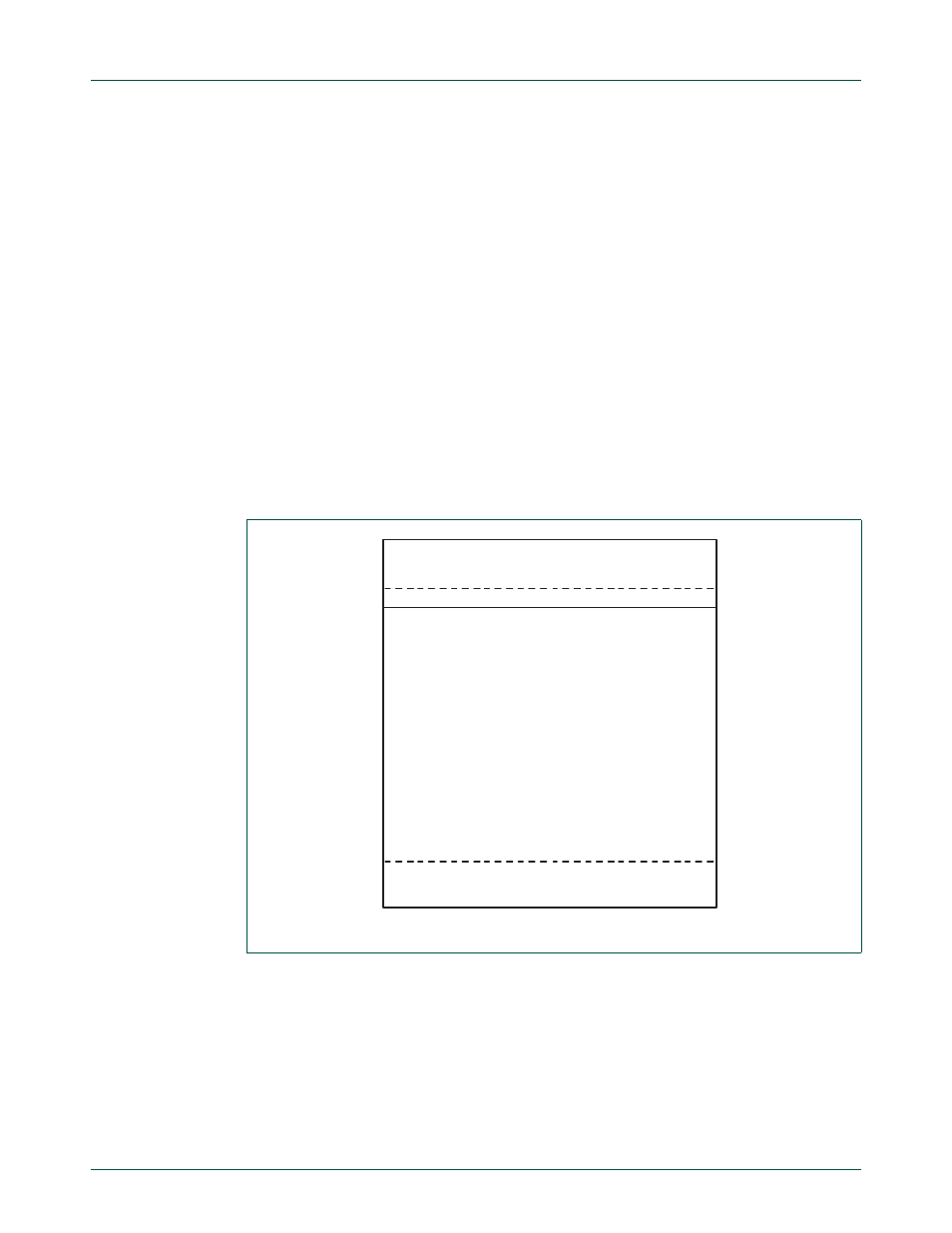
4.1 Memory map after any reset
The boot loader resides in an on-chip ROM sector of 8 kB in size. After any reset the
entire boot sector is also mapped to the top of the on-chip memory space i.e. the boot
block is also visible in the memory region starting from the address 0x7FFF E000. The
serial boot loader is designed to run from this memory area, and both the ISP and IAP
software use parts of the on-chip RAM. The RAM usage is described later in this chapter.
In addition, the bottom 64 byte of the ROM boot sector are also visible in the memory
region starting from address 0x0000 0000, i.e. the interrupt vectors are mapped to the
boot ROM sector. The reset vector contains a jump instruction to the entry point of the
serial boot loader software.
4.2 Communication protocol
All ISP commands should be sent as single ASCII strings. Strings should be terminated
with Carriage Return (CR) and/or Line Feed (LF) control characters. Extra
strings. Data is sent and received in UU-encoded format.
Fig 141. Map of lower memory after reset for flashless LPC2400 parts
8 kB BOOT BLOCK
0.0 GB
ACTIVE INTERRUPT VECTORS
FROM THE BOOT BLOCK
0x7FFF FFFF
2.0 GB - 8 kB
2.0 GB
(BOOT BLOCK INTERRUPT VECTORS)
0x0000 0000
0x7FFF E000