8 look-up table programming guidelines, Figure 18–93, Nxp semiconductors – NXP Semiconductors LPC24XX UM10237 User Manual
Page 524
UM10237_4
© NXP B.V. 2009. All rights reserved.
User manual
Rev. 04 — 26 August 2009
524 of 792
NXP Semiconductors
UM10237
Chapter 18: LPC24XX CAN controllers CAN1/2
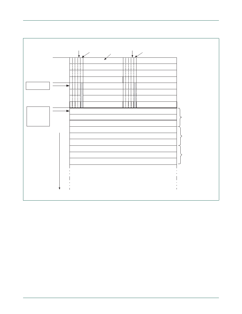
18.8 Look-up table programming guidelines
All identifier sections of the ID Look-up Table have to be programmed in such a way, that
each active section is organized as a sorted list or table with an increasing order of the
Source CAN Channel (SCC) together with CAN Identifier in each section.
SCC value equals CAN_controller - 1, i.e., SCC = 0 matches CAN1 and SCC = 1
matches CAN2.
In cases, where a syntax error in the ID Look-up Table is encountered, the Look-up Table
address of the incorrect line is made available in the Look-up Table Error Address
Register (LUTerrAd).
The reporting process in the Look-up Table Error Address Register (LUTerrAd) is a
“run-time” process. Only those address lines with syntax error are reported, which were
passed through the acceptance filtering process.
The following general rules for programming the Look-up Table apply:
Fig 93. ID Look-up table configuration example (FullCAN activated and enabled)
15
0
SCC
0
14
0
SCC
0
...
...
FullCAN
Explicit
Standard
Frame
Format
Identifier
Section
Explicit
Standard
Frame
Format
Identifier
Section
SFF_sa
= 0x10
FF RTR SEM DLC CAN-ID
FullCAN
Message
Object
section
Section
ENDofTable =
SFF_GRP_sa =
EFF_sa =
EFF_GRP_sa =
0x20
RXDATA 4, 3, 2, 1
RXDATA 8, 7, 6, 5
No Message Data, disabled.
No Message Data, disabled.
No Message Data, disabled.
FF RTR SEM DLC CAN-ID
RXDATA 4, 3, 2, 1
RXDATA 8, 7, 6, 5
Message Object
Data 0
Message Object
Data 1
Message Object
Data 2
Index
FullCAN
Interrupt
Enable bit
FullCAN
Interrupt
Enable bit
0
0
SCC
0
Disabled, 1
1
SCC
1
2
0
SCC
1
4
0
SCC
1
6
0
SCC
1
3
0
SCC
0
5
0
SCC
0
7
0
SCC
0
12
0
SCC
0
11
0
SCC
0
13
0
SCC
0
10
0
SCC
0
8
0
SCC
0
9
0
SCC
0
Message
Disable bit
Message
Disable bit
MSB
ID28
MSB
ID28
MSB
ID28
MSB
ID28
MSB
ID28
MSB
ID28
MSB
ID28
MSB
ID28
MSB
ID28
MSB
ID28
MSB
ID28
MSB
ID28
MSB
ID28
MSB
ID28
MSB
ID28
MSB
ID28
LSB
ID18
LSB
ID18
LSB
ID18
LSB
ID18
LSB
ID18
LSB
ID18
LSB
ID18
LSB
ID18
LSB
ID18
LSB
ID18
LSB
ID18
LSB
ID18
LSB
ID18
LSB
ID18
LSB
ID18
LSB
ID18