2 instruction latches and data latches, 3 flash programming issues, Memory accelerator module operating modes – NXP Semiconductors LPC24XX UM10237 User Manual
Page 103: Nxp semiconductors
UM10237_4
© NXP B.V. 2009. All rights reserved.
User manual
Rev. 04 — 26 August 2009
103 of 792
NXP Semiconductors
UM10237
Chapter 6: LPC24XX Memory Accelerator Module (MAM)
4.2 Instruction latches and data latches
Code and Data accesses are treated separately by the Memory Accelerator Module.
There is a 128 bit Latch, a 15 bit Address Latch, and a 15 bit comparator associated with
each buffer (prefetch, branch trail, and data). Each 128 bit latch holds 4 words (4 ARM
instructions, or 8 Thumb instructions).
Also associated with each buffer are 32 4:1 Multiplexers that select the requested word
from the 128 bit line.
4.3 Flash programming Issues
Since the Flash memory does not allow accesses during programming and erase
operations, it is necessary for the MAM to force the CPU to wait if a memory access to a
Flash address is requested while the Flash module is busy. (This is accomplished by
asserting the ARM7TDMI-S local bus signal CLKEN.) Under some conditions, this delay
could result in a Watchdog time-out. The user will need to be aware of this possibility and
take steps to ensure that an unwanted Watchdog reset does not cause a system failure
while programming or erasing the Flash memory.
In order to preclude the possibility of stale data being read from the Flash memory, the
LPC2400 MAM holding latches are automatically invalidated at the beginning of any Flash
programming or erase operation. Any subsequent read from a Flash address will cause a
new fetch to be initiated after the Flash operation has completed.
5.
Memory Accelerator Module operating modes
Three modes of operation are defined for the MAM, trading off performance for ease of
predictability:
Mode 0: MAM off. All memory requests result in a Flash read operation (see note 2
below). There are no instruction prefetches.
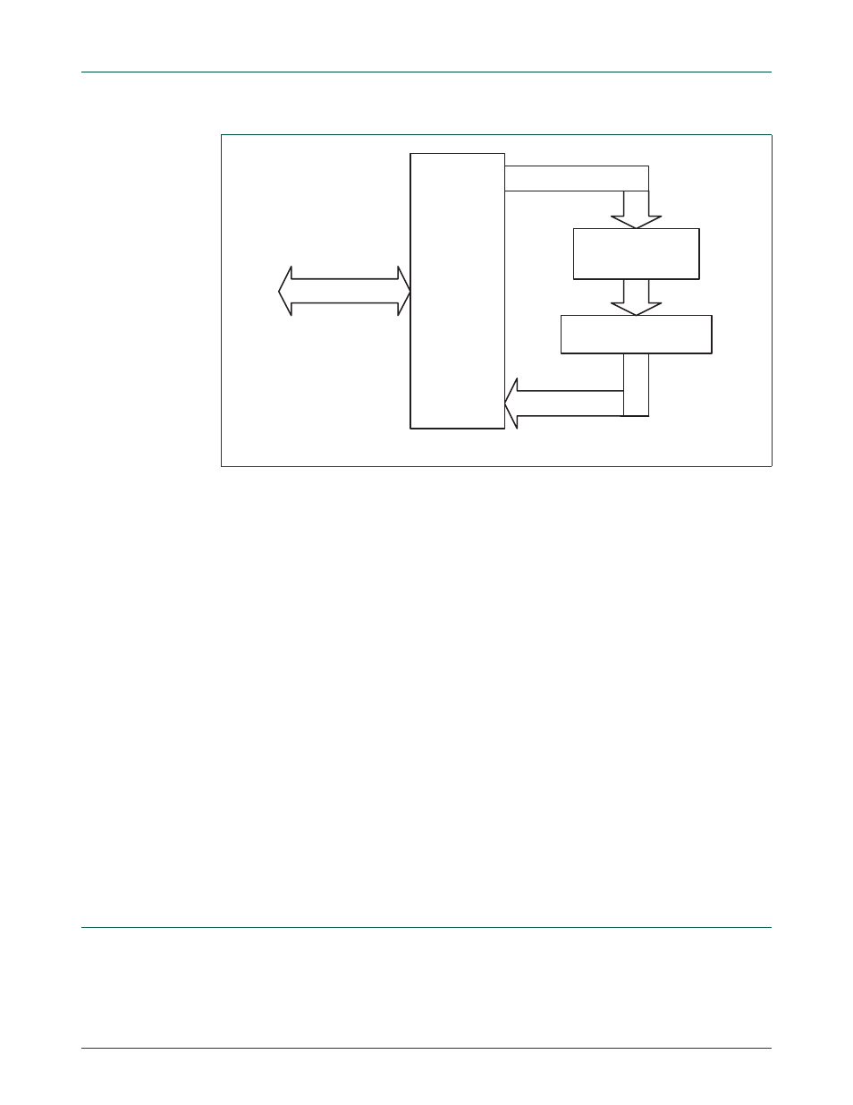
Fig 20. Simplified block diagram of the Memory Accelerator Module
BUS
INTERFACE
BUFFERS
MEMORY ADDRESS
ARM LOCAL BUS
FLASH MEMORY BANK