Nxp semiconductors, 1 ahb slave interface, 2 control logic and register bank – NXP Semiconductors LPC24XX UM10237 User Manual
Page 713: 3 dma request and response interface
UM10237_4
© NXP B.V. 2009. All rights reserved.
User manual
Rev. 04 — 26 August 2009
713 of 792
NXP Semiconductors
UM10237
Chapter 32: LPC24XX General Purpose DMA (GPDMA) controller
example, a bidirectional port requires one stream for transmit and one for receive. The
source and destination areas can each be either a memory region or a peripheral, and
can be accessed through the AHB master.
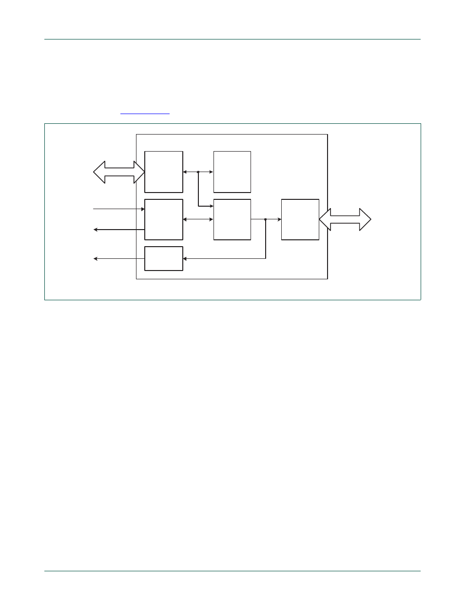
shows a block diagram of the GPDMA.
The functions of the GPDMA are described in the following sections:
•
AHB slave interface
•
Control logic and register bank
•
DMA request and response interface
•
Channel logic and channel register bank
•
Interrupt request
•
AHB master interface
•
Channel hardware
•
DMA request priority
4.2.1 AHB Slave Interface
All transactions on the AHB slave programming bus of the GPDMA are 32 bit wide.
4.2.2 Control Logic and Register Bank
The register block stores data written, or to be read across the AHB interface.
4.2.3 DMA Request and Response Interface
See DMA Interface description for information on the DMA request and response
interface.
Fig 144. GPDMA block diagram
GPDMA
AHB SLAVE
INTERFACE
CONTROL
LOGIC AND
REGISTERS
DMA
REQUEST
AND
RESPONSE
INTERFACE
CHANNEL
LOGIC AND
REGISTERS
INTERRUPT
REQUEST
AHB
MASTER
INTERFACE
DMA
requests
DMA
responses
DMA
Interrupts
AHB BUS
AHB BUS