Architecture, Pin description, Nxp semiconductors – NXP Semiconductors LPC24XX UM10237 User Manual
Page 648
UM10237_4
© NXP B.V. 2009. All rights reserved.
User manual
Rev. 04 — 26 August 2009
648 of 792
NXP Semiconductors
UM10237
Chapter 26: LPC24XX Real-Time Clock (RTC) and battery RAM
and resume operation. The alarm output has a nominal voltage swing of 1.8 V. Note that
the PLL is disabled when waking up from power-down. See
for the PLL
start-up procedure.
4.
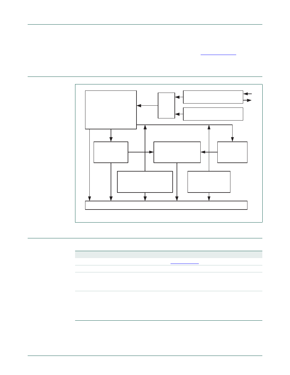
Architecture
5.
Pin description
Fig 134. RTC block diagram
CCLK
INTERRUPT GENERATOR
COUNTER INCREMENT
INTERRUPT ENABLE
ALARM MASK
REGISTER
counter
enables
CLK1
REFERENCE CLOCK DIVIDER
(PRESCALER)
CLK32k
strobe
COMPARATORS
CLOCK GENERATOR
ALARM
REGISTERS
TIME COUNTERS
RTC OSCILLATOR
MUX
Table 565. RTC pin description
Name
Type
Description
ALARM
O
Alarm output (see
).
RTCX1
I
Input to the RTC oscillator circuit.
RTCX2
O
Output from the RTC oscillator circuit.
Remark:
If the RTC is not used, the RTCX1/2 pins can be left
floating.
VBAT
I
RTC power supply:
3.3 V on this pin supplies the power to the
RTC.
Remark:
If the RTC is used, VBAT must be connected to either pin
V
DD(3V3)
, V
DD(DCDC)(3V3)
, or an independent power supply (external
battery). Otherwise, VBAT should be left floating.