1 device clock request signals, Nxp semiconductors, Chapter 15: lpc24xx usb otg controller – NXP Semiconductors LPC24XX UM10237 User Manual
Page 420
UM10237_4
© NXP B.V. 2009. All rights reserved.
User manual
Rev. 04 — 26 August 2009
420 of 792
NXP Semiconductors
UM10237
Chapter 15: LPC24XX USB OTG controller
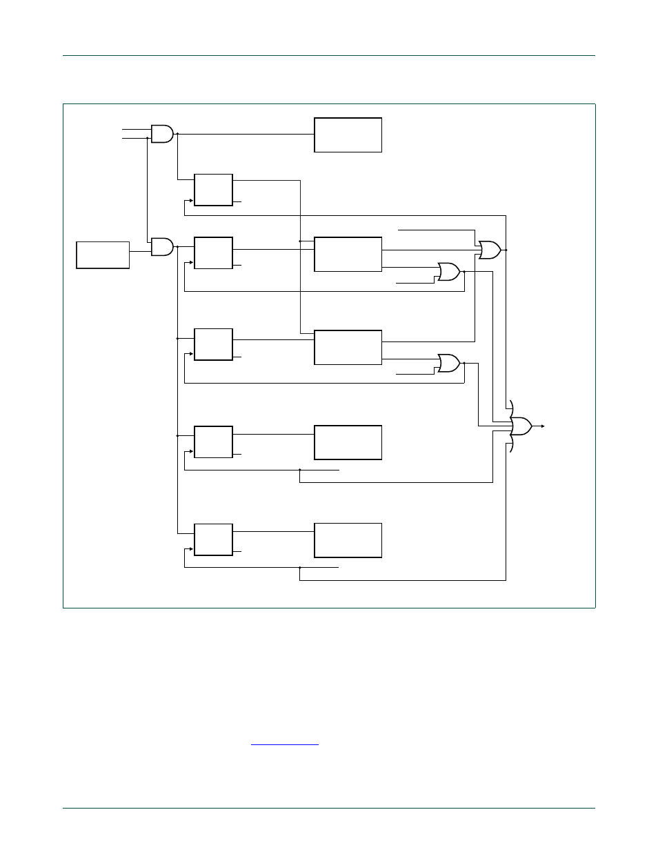
9.1 Device clock request signals
The Device controller has two clock request signals, dev_need_clk and
dev_dma_need_clk. When asserted, these signals turn on the device’s 48 MHz clock and
ahb_master_clk respectively.
The dev_need_clk signal is asserted while the device is not in the suspend state, or if the
device is in the suspend state and activity is detected on the USB bus. The dev_need_clk
signal is de-asserted if a disconnect is detected (CON bit is cleared in the SIE Get Device
Status register –
). This signal allows DEV_CLK_EN to be cleared during
normal operation when software does not need to access the Device controller registers –
the Device will continue to function normally and automatically shut off its clock when it is
suspended or disconnected.
Fig 64. Clocking and power control
CLOCK
SWITCH
USB CLOCK
DIVIDER
REGISTER
INTERFACE
DEVICE
CONTROLLER
HOST
CONTROLLER
OTG
CONTROLLER
I2C
CONTROLLER
AHB_CLK_ON
ahb_slave_clk
ahb_master_clk
DEV_CLK_ON
HOST_CLK_ON
OTG_CLK_ON
I2C_CLK_ON
DEV_CLK_EN
HOST_CLK_EN
OTG_CLK_EN
I2C_CLK_EN
dev_dma_need_clk
host_dma_need_clk
dev_need_clk
host_need_clk
AHB_CLK_EN
ahb_need_clk
PCUSB
cclk
usbclk
(48 MHz)
EN
CLOCK
SWITCH
EN
CLOCK
SWITCH
EN
EN
CLOCK
SWITCH
CLOCK
SWITCH
EN
USB_NEED_CLK