FUJITSU MB91460 SERIES FR60 User Manual
Page 997
981
Chapter 52 Regulator Control
3.Registers
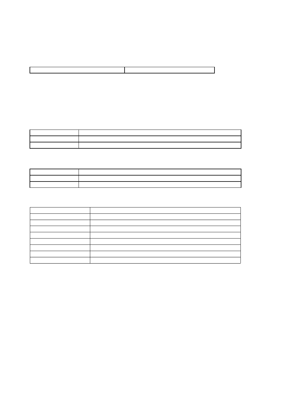
• REGSEL: Address 04CEh (Access: Byte, Halfword, Word)
Meaning of Bit Attribute Symbols (Page No.10)
” for details of the attributes.)
• Bit7-6: Reserved bit. The read value is always “0”.
• Bit5: Flash memory supply mode.
Note: Please check with the related device datasheet if this setting is supported.
• Bit4: Main Regulator supply mode.
Note: Please check with the related device datasheet if this setting is supported.
• Bit3-0: Sub-regulator voltage level
Note: The set level of the Sub-regulator voltage is only be effective in case of Main Regulator is switched
off. Otherwise (with main regulator on) the default level is applied internally by hardware to the Sub-Reg-
ulator (the register setting is not changed in this case and will be applied next time the main regulator is
switched off).
7
6
5
4
3
2
1
0
bit
-
-
FLASHSEL
MAINSEL
SUBSEL3
SUBSEL2
SUBSEL1
SUBSEL0
0
0
0
0
0
1
1
0
Initial value (
INIT pin input,
watchdog reset
)
X
X
X
X
X
X
X
X
Initial value
(Software reset)
R0/WX
R0/WX
R/W
R/W
R/W
R/W
R/W
R/W
Attribute
FLASHSEL
Function
0
Flash memory operation mode is 1.8V [Initial value]
1
Flash memory operation mode is 1.9V
MAINSEL
Function
0
Main regulator operation mode is 1.8V [Initial value]
1
Main regulator operation mode is 1.9V
SUBSEL3-SUBSEL0
Voltage level
0111
1.9V +/- 0.1V
0110
1.8V +/- 0.1V (initial)
0101
1.7V +/- 0.1V
0100
1.6V +/- 0.1V
0011
1.5V +/- 0.1V
0010
1.4V +/- 0.1V
0001
1.3V +/- 0.1V
0000
1.2V +/- 0.1V