FUJITSU MB91460 SERIES FR60 User Manual
Page 907
891
Chapter 44 A/D Converter
3.Registers of A/D Converter
Cleared by writing "0" or by a reset. (Not cleared at the end of DMA transfer.) However when waiting
condition of DMA transfer, this bit cannot be cleared.
Regarding protect function of converted data, see Section “
".
[bit 3, 2] STS1, STS0 (Start source select)
These bits initialized "00" by reset.
These bits select the A/D activation source.
In multiple-activation modes, the first activation to occur starts A/D conversion.
The activation source changes immediately on writing to the register. Therefore care is required when
switching activation mode during A/D operation.
The A/D converter detects falling edges on the external trigger pin. When external trigger level is "L" and
if these bits are changed to external trigger activation mode, A/D converting may starts.
Selecting the timer selects the 16-bit reload timer 7.
[bit 1] STRT (Start)
Writing "1" to this bit starts A/D conversion (software activation).
Write "1" again to restart conversion.
Initialized to "0" by a reset.
In continuous and stop mode, restarting is not occurred. Check BUSY bit before writing "1". (Activate
conversion after clearing.)
Do not specify forcible termination and software activation (BUSY="0" and STRT="1") at the same time.
[bit 0] reserved bit
Always write "0" to this bit.
■
A/D control status register 0 (ADCS0)
• ADCS0 (ADC0): Address 01A5h (Access:
Half-word, Byte
)
Meaning of Bit Attribute Symbols (Page No.10)
” for details of the attributes.)
[bit 7, 6] MD1, MD0 (A/D converter mode set)
These bits the operation mode.
Single mode: Continuous A/D conversion from selected channel(s) ANS4 to ANS0 to selected channel(s)
ANE4 to ANE0 with a pause after every conversion cycle.
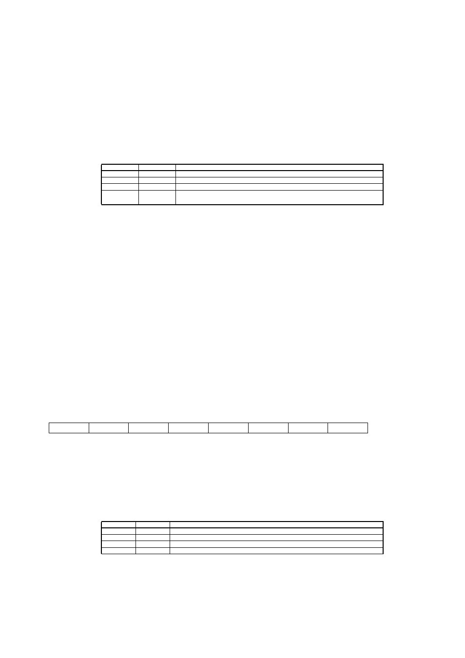
STS1
STS0
Function
0
0
Software activation [Initial value]
0
1
External trigger pin activation and software activation
1
0
Timer activation and software activation
1
1
External trigger pin activation, timer activation and software
activation
7
6
5
4
3
2
1
0
Bit
MD1
MD0
S10
ACH4
ACH3
ACH2
ACH1
ACH0
0
0
0
0
0
0
0
0
Initial
value
R/W
R/W
R/W
R
R
R
R
R
Attribute
MD1
MD0
Operating mode
0
0
Single mode ; all restarts conversion during operation enabled
0
1
Single mode ; restarts conversion during operation disabled
1
0
Continuous mode ; restarts conversion during operation disabled
1
1
Stop mode ; restarts conversion during operation disabled