FUJITSU MB91460 SERIES FR60 User Manual
Page 454
438
Chapter 30 I/O Ports
1.I/O Ports Functions
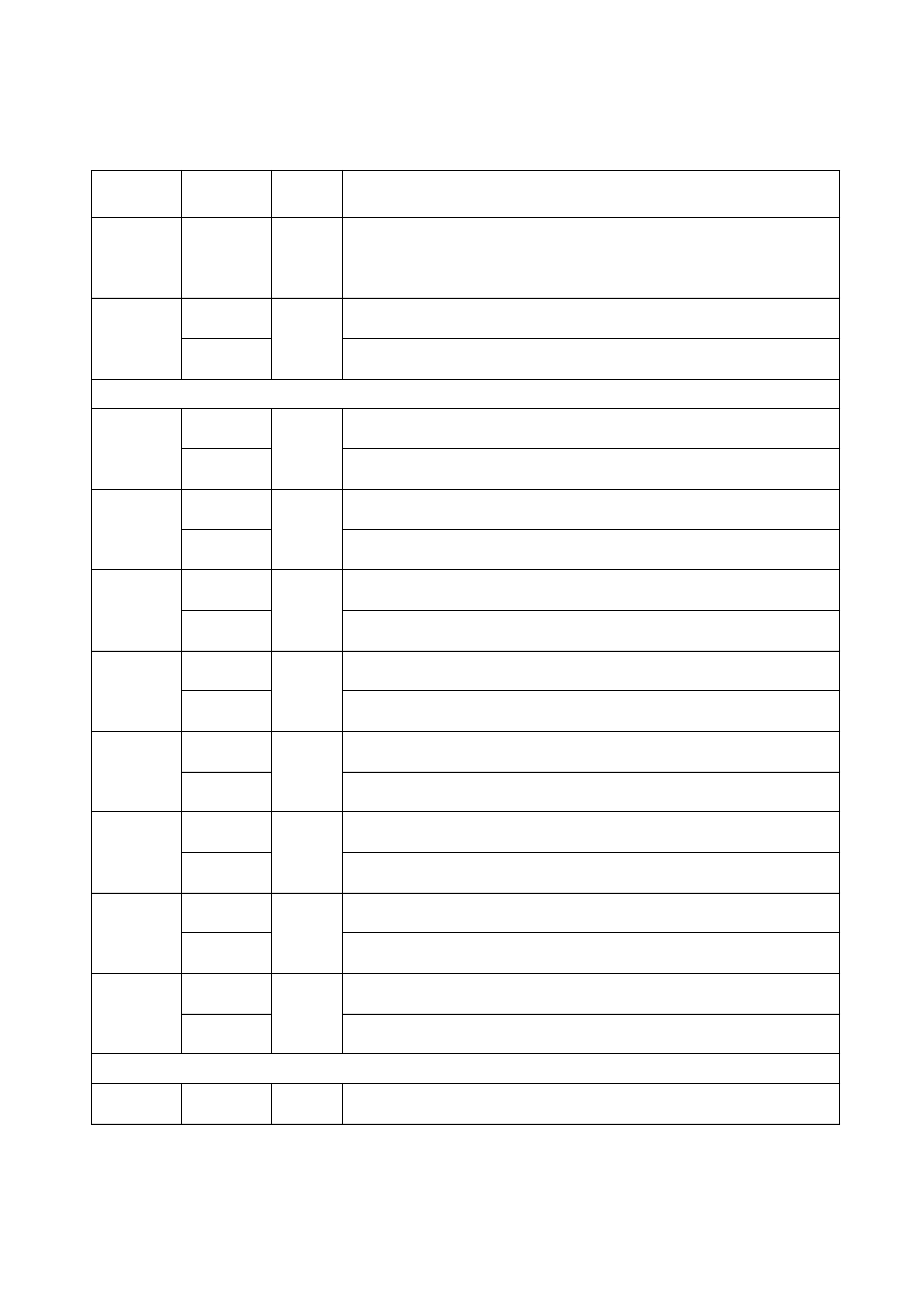
P08_1
P08_1
TP04_0
General purpose I/O. This function is enabled in the single-chip mode or by
setting the corresponding PFR to ‘0’.
WRX1
Output pin for external bus write strobe. This function is enabled when the
external bus is enabled.
P08_0
P08_0
TP04_0
General purpose I/O. This function is enabled in the single-chip mode or by
setting the corresponding PFR to ‘0’.
WRX0
Output pin for external bus write strobe. This function is enabled when the
external bus is enabled.
Port 09
P09_7
P09_7
TP04_0
General purpose I/O. This function is enabled in the single-chip mode or by
setting the corresponding PFR to ‘0’.
CSX7
Output pin for external bus chip select area 7. This function is enabled when
the external bus is enabled.
P09_6
P09_6
TP04_0
General purpose I/O. This function is enabled in the single-chip mode or by
setting the corresponding PFR to ‘0’.
CSX6
Output pin for external bus chip select area 6. This function is enabled when
the external bus is enabled.
P09_5
P09_5
TP04_0
General purpose I/O. This function is enabled in the single-chip mode or by
setting the corresponding PFR to ‘0’.
CSX5
Output pin for external bus chip select area 5. This function is enabled when
the external bus is enabled.
P09_4
P09_4
TP04_0
General purpose I/O. This function is enabled in the single-chip mode or by
setting the corresponding PFR to ‘0’.
CSX4
Output pin for external bus chip select area 4. This function is enabled when
the external bus is enabled.
P09_3
P09_3
TP04_0
General purpose I/O. This function is enabled in the single-chip mode or by
setting the corresponding PFR to ‘0’.
CSX3
Output pin for external bus chip select area 3. This function is enabled when
the external bus is enabled.
P09_2
P09_2
TP04_0
General purpose I/O. This function is enabled in the single-chip mode or by
setting the corresponding PFR to ‘0’.
CSX2
Output pin for external bus chip select area 2. This function is enabled when
the external bus is enabled.
P09_1
P09_1
TP04_0
General purpose I/O. This function is enabled in the single-chip mode or by
setting the corresponding PFR to ‘0’.
CSX1
Output pin for external bus chip select area 1. This function is enabled when
the external bus is enabled.
P09_0
P09_0
TP04_0
General purpose I/O. This function is enabled in the single-chip mode or by
setting the corresponding PFR to ‘0’.
CSX0
Output pin for external bus chip select area 0. This function is enabled when
the external bus is enabled.
Port 10
P10_7
P10_7
TP04_0
General purpose I/O. This function is enabled in the single-chip mode or by
setting the corresponding PFR to ‘0’.
Pin Name
I/O Signal
Circuit
Type
Function