Block diagram of a/d converter – FUJITSU MB91460 SERIES FR60 User Manual
Page 902
886
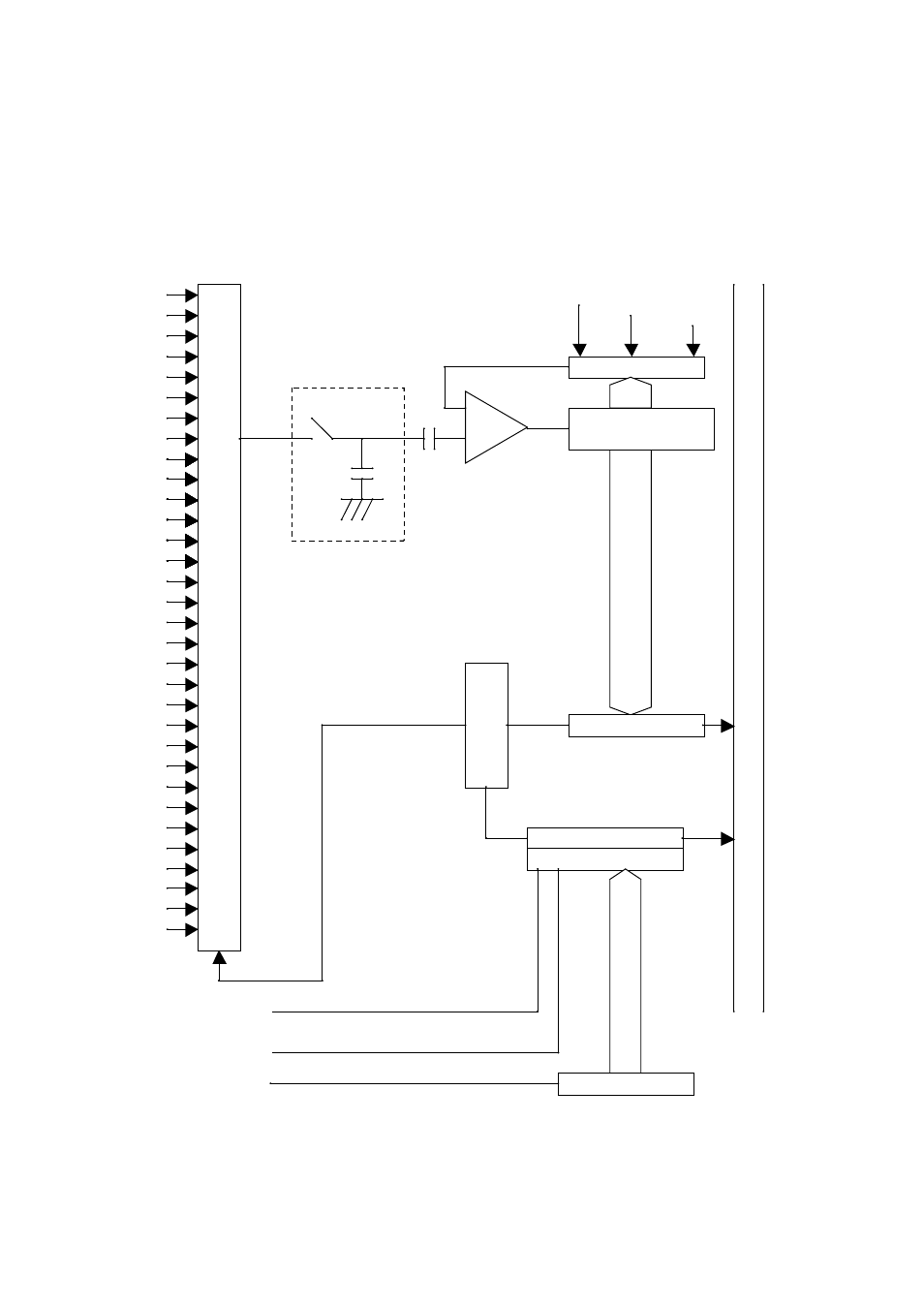
Chapter 44 A/D Converter
2.Block Diagram of A/D Converter
2. Block Diagram of A/D Converter
Following figure shows block diagram of A/D converter.
Block diagram of A/D converter
Figure 2-1 Figure 20.2-1 "Block Diagram of A/D Converter"
AVSS
AVRH/ L
AVCC
CLKP
O pe rat in g
Clo c k
ADC S 0/ 1
in
p
u
t
c
ir
c
u
it
AN0
AN1
AN2
AN3
AN4
AN5
AN6
AN7
AN8
AN9
AN10
AN11
AN12
AN13
AN14
AN15
AN16
AN17
AN18
AN19
AN20
AN21
AN22
AN23
AN24
AN25
AN26
AN27
AN28
AN29
AN30
AN31
MP X
D/ A co n ve rte r
Sample & Hold
c irc uit
Comparat or
D
eco
d
e
r
A/ D dat a re gis te r
Da
ta
b
u
s
A/ D co nt ro l re gis t er 0
A/ D co nt ro l re gis t er 1
ATGX
1 6- bit
Re lo ad Time r
P re sc ale r
S e quen t ial
c o mpariso n re gis t er
See also other documents in the category FUJITSU Hardware:
- XG Series P3NK-4452-01ENZD (614 pages)
- FPCAC14C (1 page)
- MCJ3230SS (161 pages)
- MBA3073NC (138 pages)
- T5140 (76 pages)
- T5140 (102 pages)
- MAM3367MC/MP (152 pages)
- MPC3045AH (185 pages)
- MB2142-02 (23 pages)
- MB15F86UL (6 pages)
- MHS2030AT (40 pages)
- MHW2100BS (296 pages)
- MHK2060AT (227 pages)
- Disk Drives MHK2060AT (227 pages)
- MCM3064SS (170 pages)
- Mainboard D1561 (45 pages)
- MHC2040AT (219 pages)
- D1961 (45 pages)
- DISK DRIVES MHM2100AT (231 pages)
- MHR2010AT (250 pages)
- MHZ2120BJ (320 pages)
- MCE3064AP (175 pages)
- LQFP-64P (16 pages)
- Solaris PCI GigabitEthernet 3.0 (115 pages)
- MAY2036RC (94 pages)
- MAB3091 (142 pages)
- MPE3XXXAT (191 pages)
- MHV2040AH (40 pages)
- MHW2040AC (278 pages)
- ETERNUSmgr P2X0-0202-01EN (64 pages)
- VSS Hardware Provider 2.1 (134 pages)
- MAG3182FC (61 pages)
- MAU3147NC/NP (130 pages)
- MAX3147RC (94 pages)
- MHV2160BT (296 pages)
- MHV2040AT (280 pages)
- MAW3300NC/NP (130 pages)
- DeskPower E623 (50 pages)
- MAG3182LC (133 pages)
- OPTICAL DISK DRIVES MDG3064UB (42 pages)
- MHF2021AT (225 pages)
- MHR2040AT (40 pages)
- Single Drive FTM7926FB (1 page)
- PG-FCS103 (98 pages)
- MAS3735FC (114 pages)