Registers, 1 clkr: clock source control register, Registers 4.1 clkr: clock source control register – FUJITSU MB91460 SERIES FR60 User Manual
Page 207
191
Chapter 13 Clock Control
4.Registers
4. Registers
4.1 CLKR: Clock Source Control Register
Selects the clock source for the base clock used to run the MCU and controls the PLL.
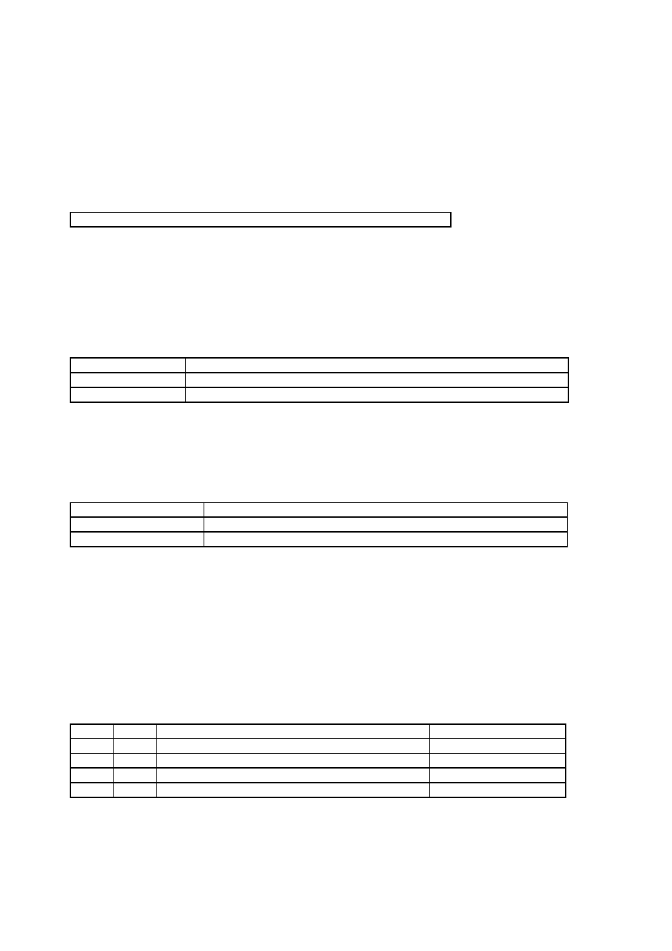
• CLKR: Address 0484h (Access: Byte)
Meaning of Bit Attribute Symbols (Page No.10)
” for details of the attributes.)
• Bit7-4: Reserved bitAlways write “0” to this bit. The read value is the value written.
• Bit3: Subclock select enable
• Modifying the subclock selection enable bit (SCKEN) while the subclock is selected as the clock source
(CLKS[1:0]=“11”) is prohibited (result is not guaranteed). Only modify the setting when the main clock is
selected.
(See the explanation for the clock source selection bits (CLKS[1:0]) for details of how to change the clock
source.)
• Bit2: Enable main PLL operation
• Modifying the main PLL operation enable bit (PLL1EN) while the main PLL is selected as the clock
source (CLKS[1:0]=“10”) is prohibited.
• Modifying the main PLL operation enable bit (PLL1EN) while the clock autogear function is active (gear
up or gear down) is prohibited. Always check the gear status flags before changing the PLL state (see
chapter
"Clock Auto Gear Up/Down" on P. 213
).
• If the main clock oscillation is halted (STCR.OSCD1=“1”), the main PLL halts during stop mode even if
the PLL enable bit (PLL1EN) is set to “1”. If main PLL operation is enabled (PLL1EN=“1”), the main clock
operates using the PLL after recovering from stop mode.
(See the explanation for the clock source selection bits (bits 1-0:) for details of changing the clock
source.)
• Bit1-0: Clock source selection
• When changing the clock mode, the value of CLKS0 may not be modified while CLKS1 is “1”.
The table below lists the cases in which the CLKS1- CLKS0 bits may be modified.
• There is no setting to select the subclock divided by 2.
7
6
5
4
3
2
1
0
bit
-
-
-
-
SCKEN
PLL1EN
CLKS1
CLKS0
X
X
X
X
0
0
0
0
Initial value (
INIT pin input,
watchdog reset
)
X
X
X
X
X
X
X
X
Initial value
(Software reset)
R/W0
R/W0
R/W0
R/W0
R/W
R/W
R/W
R/W
Attribute
SCKEN
Function
0
Prohibit subclock selection [Initial value]
1
Enable subclock selection
PLL1EN
Function
0
Halt main PLL (Initial value)
1
Enable main PLL operation
CLKS1
CLKS0
Clock source setting
Mode
0
0
Main clock input from X0/X1 divided by 2 (Initial value)
Main clock mode
0
1
Main clock input from X0/X1 divided by 2
Main clock mode
1
0
Main PLL
Main clock mode
1
1
Subclock
Subclock mode