Register, 1 clock monitor configuration register, Register 4.1 clock monitor configuration register – FUJITSU MB91460 SERIES FR60 User Manual
Page 959
943
Chapter 48 Clock Monitor
4.Register
4. Register
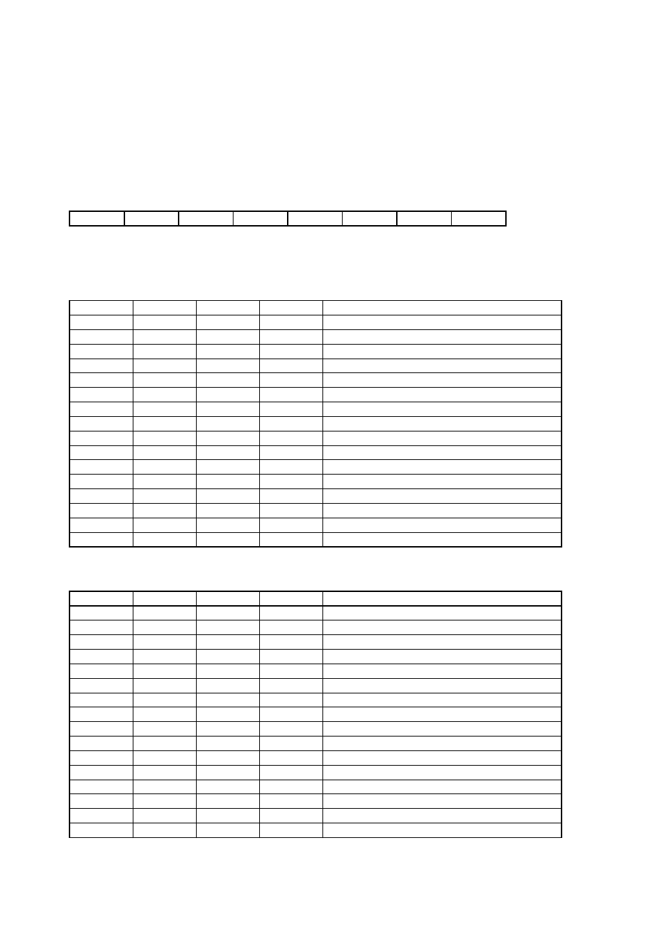
4.1 Clock Monitor Configuration Register
A register for output settings of an internal clock signal
• CMCFG: Address 04AF
H
(Access: Byte)
(For attributes, refer to “
Meaning of Bit Attribute Symbols (Page No.10)
”.)
• bit7-4: Select an output frequency prescaler
Specifies the frequency of a clock signal output to a clock monitor terminal.
• bit3-0: Select an output frequency prescaler
7
6
5
4
3
2
1
0
bit
CMPRE3
CMPRE2
CMPRE1
CMPRE0
CMSEL3
CMSEL2
CMSEL1
CMSEL0
0
0
0
0
0
0
0
0
Initial value
R/W
R/W
R/W
R/W
R/W
R/W
R/W
R/W
Attributes
CMPRE3
CMPRE2
CMPRE1
CMPRE0
Clock Frequency Output to the MONCLK pin
0
0
0
0
Source clock (selected by CMSEL) divided by 1 (Initial)
0
0
0
1
Source clock (selected by CMSEL) divided by 2
0
0
1
0
Source clock (selected by CMSEL) divided by 3
0
0
1
1
Source clock (selected by CMSEL) divided by 4
0
1
0
0
Source clock (selected by CMSEL) divided by 5
0
1
0
1
Source clock (selected by CMSEL) divided by 6
0
1
1
0
Source clock (selected by CMSEL) divided by 7
0
1
1
1
Source clock (selected by CMSEL) divided by 8
1
0
0
0
Source clock (selected by CMSEL) divided by 9
1
0
0
1
Source clock (selected by CMSEL) divided by 10
1
0
1
0
Source clock (selected by CMSEL) divided by 11
1
0
1
1
Source clock (selected by CMSEL) divided by 12
1
1
0
0
Source clock (selected by CMSEL) divided by 13
1
1
0
1
Source clock (selected by CMSEL) divided by 14
1
1
1
0
Source clock (selected by CMSEL) divided by 15
1
1
1
1
Source clock (selected by CMSEL) divided by 16
CMSEL
CMSEL2
CMSEL1
CMSEL0
Clock Source Output to the MONCLK pin
0
0
0
0
MONCLK output disabled (high impedance) (Initial)
0
0
0
1
Main oscillation before clock supervisor
0
0
1
0
Sub oscillation before clock supervisor
0
0
1
1
RC oscillation
0
1
0
0
Sub clock (after sub clock selector SCKS)
0
1
0
1
Main oscillation after clock supervisor (MCLK_OUT)
0
1
1
0
Sub oscillation after clock supervisor (SCLK_OUT)
0
1
1
1
Clock modulator output to Clock Control
1
0
0
0
Clock modulator observer output
1
0
0
1
PLL output after 1/g divider (Auto Gear)
1
0
1
0
PLL output after 1/m divider (PLL output)
1
0
1
1
PLL output after 1/c divider (CAN clock)
1
1
0
0
PLL input after 1/n divider (PLL feedback)
1
1
0
1
CLKB
1
1
1
0
CLKP
1
1
1
1
CLKT