FUJITSU MB91460 SERIES FR60 User Manual
Page 467
451
Chapter 30 I/O Ports
1.I/O Ports Functions
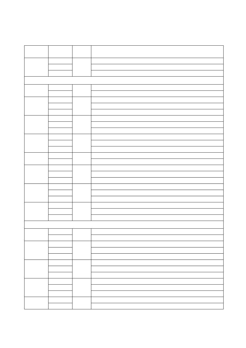
P32_0
P32_0
TP06_0
General purpose I/O.
SEG24
Segment driver output pin 24 LCD controller.
SIN14
Serial data input pin for LIN-USART 14.
Port 33
P33_7
P33_7
TP06_0
General purpose I/O.
SEG23
Segment driver output pin 23 LCD controller.
P33_6
P33_6
TP06_0
General purpose I/O.
SEG22
Segment driver output pin 22 LCD controller.
SCK13
Clock I/O pin for LIN-USART 13.
P33_5
P33_5
TP06_0
General purpose I/O.
SEG21
Segment driver output pin 21 LCD controller.
SOT13
Serial data output pin for LIN-USART 13.
P33_4
P33_4
TP06_0
General purpose I/O.
SEG20
Segment driver output pin 20 LCD controller.
SIN13
Serial data input pin for LIN-USART 13.
P33_3
P33_3
TP06_0
General purpose I/O.
SEG19
Segment driver output pin 19 LCD controller.
P33_2
P33_2
TP06_0
General purpose I/O.
SEG18
Segment driver output pin 18 LCD controller.
SCK12
Clock I/O pin for LIN-USART 12.
P33_1
P33_1
TP06_0
General purpose I/O.
SEG17
Segment driver output pin 17 LCD controller.
SOT12
Serial data output pin for LIN-USART 12.
P33_0
P33_0
TP06_0
General purpose I/O.
SEG16
Segment driver output pin 16 LCD controller.
SIN12
Serial data input pin for LIN-USART 12.
Port 34
P34_7
P34_7
TP06_0
General purpose I/O.
SEG15
Segment driver output pin 15 LCD controller.
P34_6
P34_6
TP06_0
General purpose I/O.
SEG14
Segment driver output pin 14 LCD controller.
SCK11
Clock I/O pin for LIN-USART 11.
P34_5
P34_5
TP06_0
General purpose I/O.
SEG13
Segment driver output pin 13 LCD controller.
SOT11
Serial data output pin for LIN-USART 11.
P34_4
P34_4
TP06_0
General purpose I/O.
SEG12
Segment driver output pin 12 LCD controller.
SIN11
Serial data input pin for LIN-USART 11.
P34_3
P34_3
TP06_0
General purpose I/O.
SEG11
Segment driver output pin 11 LCD controller.
Pin Name
I/O Signal
Circuit
Type
Function