FUJITSU MB91460 SERIES FR60 User Manual
Page 537
521
Chapter 31 External Bus
2.External Bus Interface Registers
The function of each bit changes according to the access type (TYP(3-0) bits) setting of the ACR0-7 registers,. A
chip select area determined by either of the following settings becomes the area for normal access or a address/
data multiplex access operation.
The following lists the functions of each AWR0-7 bit for a normal access or address/data multiplex access area.
Since the initial values of registers other than AWR0 are undefined, set them to their initial values before enabling
each area with the CSER register.
The following explains the functions of the bits in the area wait registers (AWR0-7).
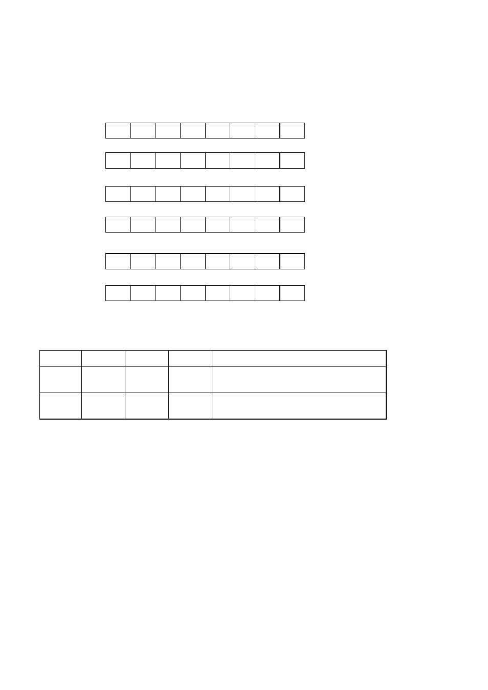
TYP3
TYP2
TYP1
TYP0
Access type
0
0
x
x
Normal access (asynchronous SRAM, I/O,
and single/page/burst-ROM/FLASH)
0
1
x
x
Address data multiplex access (8/16-bit bus
width only)
0000 066A
H
W15
W14
W13
W12
W11
W10
W09
W08
AWR5L
7
6
5
4
3
2
1
0
0000 066B
H
W07
W06
W05
W04
W03
W02
W01
W00
31
30
29
28
27
26
25
24
0000 066C
H
W15
W14
W13
W12
W11
W10
W09
W08
0000 066D
H
W07
W06
W05
W04
W03
W02
W01
W00
0000 066E
H
W15
W14
W13
W12
W11
W10
W09
W08
7
6
5
4
3
2
1
0
0000 066F
H
W07
W06
W05
W04
W03
W02
W01
W00
23
22
21
20
19
18
17
16
15 14 13 12 11 10 9 8
15 14 13 12 11 10 9 8
AWR5H
AWR6L
AWR6H
AWR7L
AWR7H
xxxxxxxx
b
xxxxxxxx
b
xxxxxxxx
b
xxxxxxxx
b
xxxxxxxx
b
xxxxxxxx
b
xxxxxxxx
b
xxxxxxxx
b
xxxxxxxx
b
xxxxxxxx
b
W/R
W/R
W/R
W/R
W/R
xxxxxxxx
b
xxxxxxxx
b
W/R
Initial value
INIT RST Access