FUJITSU MB91460 SERIES FR60 User Manual
Page 262
246
Chapter 17 Clock Modulator
2.Clock Modulator Registers
Note: NOT ALL SETTINGS ARE ALLOWED ON EVERY DEVICE!
Please consider the actual maximal allowed clock frequency of the MCU (refer to the data sheet).
F0:
Frequency of unmodulated input clock (PLL frequency)
T0:
Period of unmodulated input clock (PLL clock period)
resolution:
resolution of frequencies in the modulated clock. low (1) to high (7)
F
min
:
minimal frequency occurring in the frequency modulated clock
F
max
:
maximal frequency occurring in the frequency modulated clock
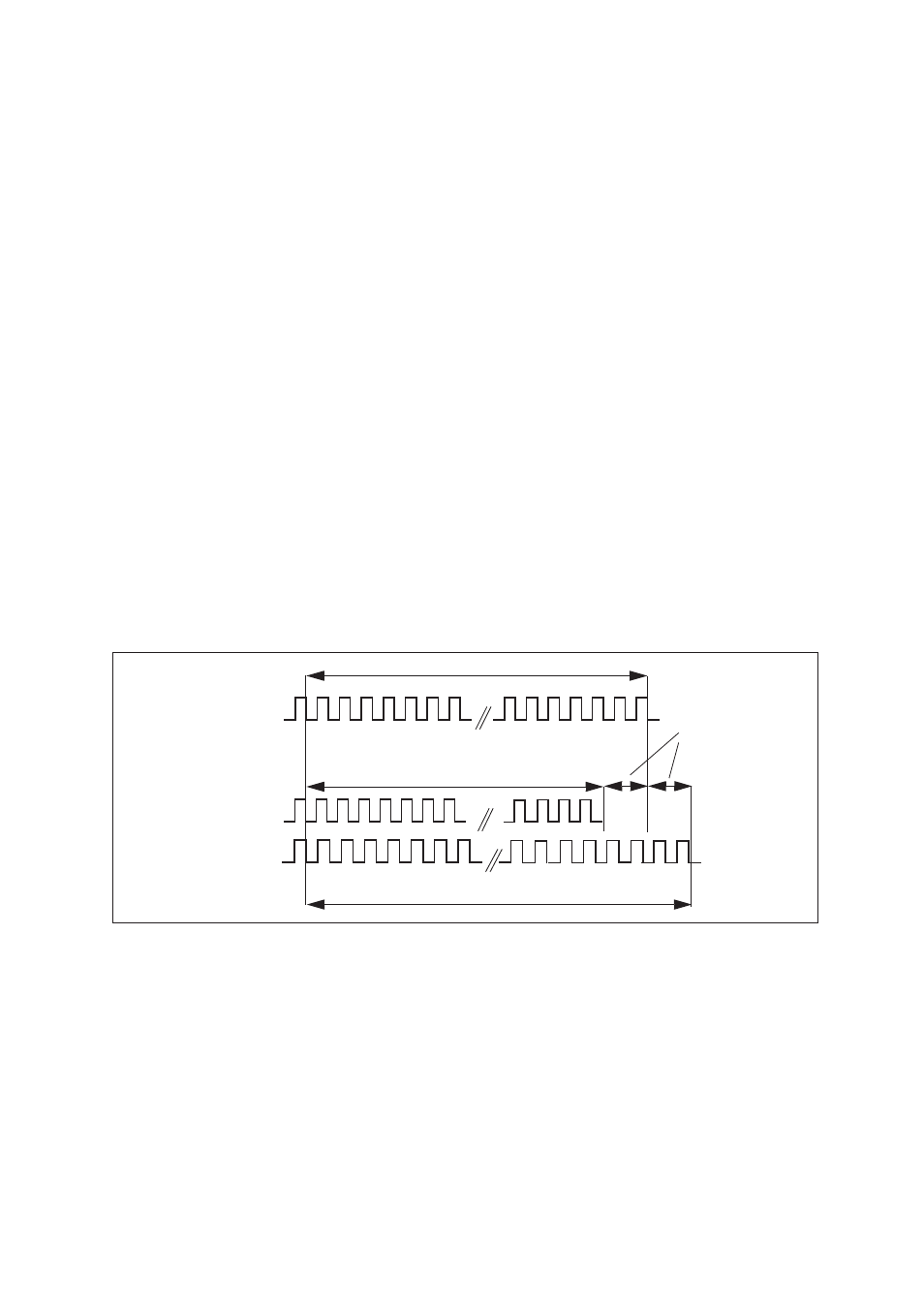
phase skew:
The maximal phase shift of the modulated clock relative to the unmodulated
reference clock in terms of clock periods of the unmodulated clock.
Example: phase skew=1.44
In worst case, a sequence of n periods of the modulated clock can be 1.44*T0
shorter or 1.44*T0 longer than a sequence of n periods of the unmodulated
reference clock.
n can be any number > 50 periods
phase skew 50:
phase skew for sequences with n<= 50 periods
CMPR:
register setting of the CMPR register
n periods
n periods
n periods
reference clock
modulated clock
phase skew
+
-