4 gcn1: general control register 1 – FUJITSU MB91460 SERIES FR60 User Manual
Page 820
804
Chapter 39 Programmable Pulse Generator
4.Registers
4.4 GCN1: General Control register 1
Selects a trigger input to PPG0-PPG3, PPG4-PPG7, PPG8-PPG11 and PPG12-PPG15.
• GCN10 (PPG0-PPG3): Address 0100h (Access:
Half-word
)
• GCN11 (PPG4-PPG7): Address 0104h (Access:
Half-word
)
• GCN12 (PPG8-PPG11): Address 0108h (Access:
Half-word
)
• GCN13 (PPG12-PPG15): Address 0320h (Access:
Half-word
)
Meaning of Bit Attribute Symbols (Page No.10)
” for details of the attributes.)
PPG12-PPG15:
•GCN13: Bits 15-12
(TSEL3[3:0])
PPG15 trigger specification
•GCN13: Bits 11-8
(TSEL2[3:0])
PPG14 trigger specification
•GCN13: Bits 7-4
(TSEL1[3:0])
PPG13 trigger specification
•GCN13: Bits 3-0
(TSEL0[3:0])
PPG12 trigger specification
PPG8-PPG11:
•GCN12: Bits 15-12
(TSEL3[3:0])
PPG11 trigger specification
•GCN12: Bits 11-8
(TSEL2[3:0])
PPG10 trigger specification
•GCN12: Bits 7-4
(TSEL1[3:0])
PPG9 trigger specification
•GCN12: Bits 3-0
(TSEL0[3:0])
PPG8 trigger specification
PPG4-PPG7:
•GCN11: Bits 15-12
(TSEL3[3:0])
PPG7 trigger specification
•GCN11: Bits 11-8
(TSEL2[3:0])
PPG6 trigger specification
•GCN11: Bits 7-4
(TSEL1[3:0])
PPG5 trigger specification
•GCN11: Bits 3-0
(TSEL0[3:0])
PPG4 trigger specification
PPG0-PPG3:
•GCN10: Bits 15-12
(TSEL3[3:0])
PPG3 trigger specification
•GCN10: Bits 11-8
(TSEL2[3:0])
PPG2 trigger specification
•GCN10: Bits 7-4
(TSEL1[3:0])
PPG1 trigger specification
•GCN10: Bits 3-0
(TSEL0[3:0])
PPG0 trigger specification
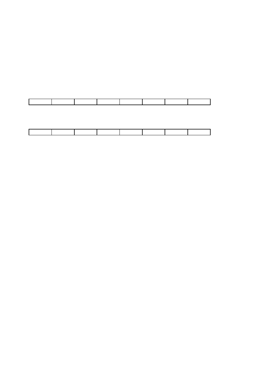
15
14
13
12
11
10
9
8
Bit
TSEL33
TSEL32
TSEL31
TSEL30
TSEL23
TSEL22
TSEL21
TSEL20
0
0
1
1
0
0
1
0
Initial value
R/W
R/W
R/W
R/W
R/W
R/W
R/W
R/W
Attribute
7
6
5
4
3
2
1
0
Bit
TSEL13
TSEL12
TSEL11
TSEL10
TSEL03
TSEL02
TSEL01
TSEL00
0
0
0
1
0
0
0
0
Initial value
R/W
R/W
R/W
R/W
R/W
R/W
R/W
R/W
Attribute