FUJITSU MB91460 SERIES FR60 User Manual
Page 617
601
Chapter 31 External Bus
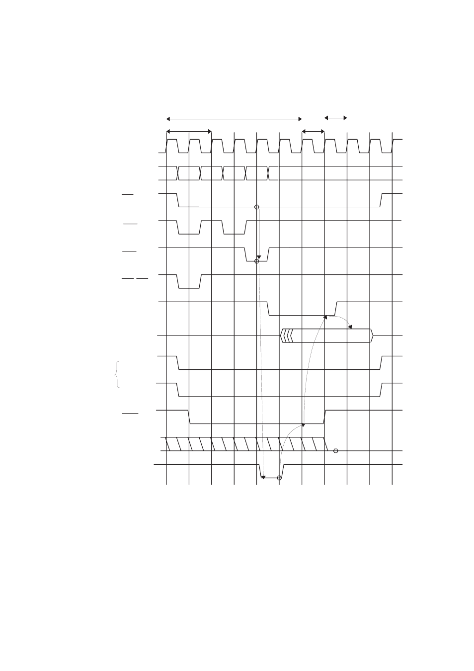
10.DMA Access Operation
Signal (CL = 2)
The rise of the IOWR signal can be delayed one cycle by extending SDRAM read access one cycle when the
signal resulting from OR (negative - logic AND) operation of the CAS signal and the chip select signal for the
SDRAM area subject to transfer is input t
As the external wait signal is generated based on the CAS signal rise timing in this case, the data setup time from
the SDRAM data output to the I/O device can be reserved for one cycle, regardless of a page hit or miss in
SDRAM.
Set the external wait using the RYE0 and RYE1 bits in the DMAC I/O wait register such that the RDY function of
the DMA fly - by access channel to be used is enabled.
When the CAS latency is 3, SDRAM data output is delayed one cycle. Add one stage of FF by the MCLK to input
the signal delayed one cycle from the above diagram to the RDY pin.
SDRAM basic access
I/O hold
wait
External RDY wait
I/O basic cycle
MCLK
A31 to 0
CSn
SRAS
SCAS
WRn(SWE)
MCLKE
D31 to 0
DACKn
DEOPn
IOWR
DREQn
RDY
Basic mode
Bank
Address
Column
Address
Row
Address