FUJITSU MB91460 SERIES FR60 User Manual
Page 1031
1015
Chapter 55 Flash Security
4.Register
• Bit31-25: Reserved bit. The read value is always “0”.
• Bit24: RDY: CRC32 Sequence Ready
• Bit23-20: Reserved bit. The read value is always “0”.
• Bit19-16: CSZ3-0: CRC32 Size Mask
Remark: CSZ3-0 is used as an OR-mask for the address given by CSA15-0. See address calculation below.
• Bit15-0: CSA15-0: CRC32 Start Address
This register contains the CRC32 startaddress which is aligned to 4kByte addresses. It is only possible to
calculate the CRC32 checksum over addresses located in the Flash Memory address space. Other addresses
are invalid and might lead to wrong checksums.
Remark: The addresses to be written in this register are flash memory addresses like used in the flash parallel
programming mode and not the mapped addresses which are used in CPU mode.
■
Calculation of the CRC32 start- and end-address:
The CSZ3-0 setting is first translated into a mask value:
CRC32 Startaddress = CSA[15:0] << 12 + 0x000
CRC32 Endaddress = (CSA[15:0] or MASK ) << 12 + 0xFFF
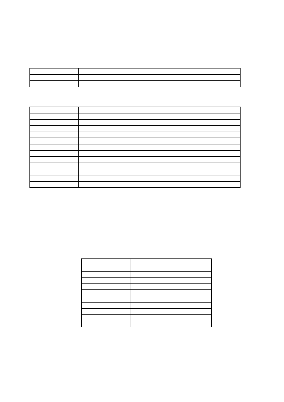
RDY
Function
0
CRC32 sequence running or not yet started
1
CRC32 sequence ready (data in the FSCR0 register is valid)
CSZ3-0
Function
0000
CRC32 sequence size mask is 4 kByte
0001
CRC32 sequence size mask is 8 kByte
0010
CRC32 sequence size mask is 16 kByte
0011
CRC32 sequence size mask is 32 kByte
0100
CRC32 sequence size mask is 64 kByte
0101
CRC32 sequence size mask is 128 kByte
0110
CRC32 sequence size mask is 256 kByte
0111
CRC32 sequence size mask is 512 kByte
1000
CRC32 sequence size mask is 1024 kByte
1001
CRC32 sequence size mask is 2048 kByte
1010
CRC32 sequence size mask is 4096 kByte
1011-1111
Not supported
CSZ3-0
MASK
0000
0000_0000_0000_0000
0001
0000_0000_0000_0001
0010
0000_0000_0000_0011
0011
0000_0000_0000_0111
0100
0000_0000_0000_1111
0101
0000_0000_0001_1111
0110
0000_0000_0011_1111
0111
0000_0000_0111_1111
1000
0000_0000_1111_1111
1001-1111
and so on...