2 dma fly-by transfer (memory -> i/o) – FUJITSU MB91460 SERIES FR60 User Manual
Page 610
594
Chapter 31 External Bus
10.DMA Access Operation
10.2 DMA Fly-By Transfer (Memory -> I/O)
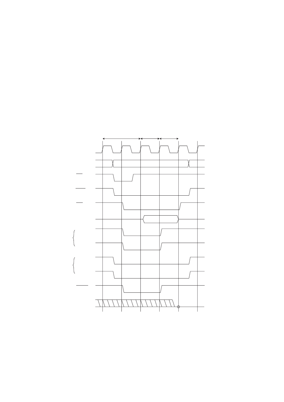
This section explains DMA fly-by transfer (memory -> I/O).
■
DMA Fly-By Transfer (Memory -> I/O)
"Timing chart for DMA Fly-By Transfer (Memory -> I/O)" shows the operation timing chart for (TYP3-
0=0000
B
, AWR=0008
H
, IOWR=41
H
).
"Timing chart for DMA Fly-By Transfer (Memory -> I/O)" shows a case in which a wait is not set on
the memory side.
Figure 10-2 Timing chart for DMA Fly-By Transfer (Memory -> I/O)
•
Setting 1 for the HLD bit of the IOWR0-3 registers extends the I/O read cycle by one cycle.
•
Setting bits WR1-0 bits of the IOWR0-3 registers enables 0-3 write recovery cycles to be inserted.
•
If the write recovery cycle is set to 1 or more, a write recovery cycle is always inserted after write access.
•
Setting bits IW3-0 of the IOWR0-3 registers enables 0-15 wait cycles to be inserted.
•
If wait is also set on the memory side (AWR15-12 is not 0), the larger value is used as the wait cycle after
comparison with the I/O wait (IW3-0 bits).
memory address
DACKn
DEOPn
DACKn
DEOPn
IORD
DREQn
MCLK
AS
CSn
A[31:0]
D[31:0]
RD
FR30
compatible
mode
Basic
mode
Sense timing in
demand mode
I/O wait I/O hold
Basic cycle cycle wait